NVIDIA HGX B300 8-GPU System Block Diagram
- 1. Interconnect Between Dual CPUs
- 1.1. Intel Platform (Xeon Scalable Series)
- 1.2. AMD Platform (EPYC Series)
- 1.3. Resources Consumed by CPU Interconnect
- 2. NUMA Architecture and PCIe Lane “Ownership”
- 2.2. PCIe Lane “Ownership”
- 2.3. Configuration Recommendations (Golden Rule)
- 3.1. Core Role: Breaking Physical Constraints for Optimal Topology
- 3.2. Addressing GPU-CPU Ratio Issues (“Peer-to-Peer” vs “Non-Peer-to-Peer” Access)
- 3.3. Enhancing Maintainability and Flexiblity (Important!)
- 4. Principles for CPU PCIe Lane Allocation to PCIe Switch
- 4.1. Typical Allocation Schemes (Mainstream Platform Example)
- 4.2. Core Allocation Principles
- 4.3. Reasons for Not Allocating All Lanes to GPUs
1. Interconnect Between Dual CPUs
CPUs are connected by a dedicated high-speed interconnect bus. This interconnect typically does not consume the PCIe lanes available for external devices, but it does use up internal bus resources on the CPU.
The interconnect technology depends on the CPU vendor and platform. Modern mainstream server interconnect technlogies include Intel’s Ultra Path Interconnect (UPI), and AMD’s Infinity Fabric.
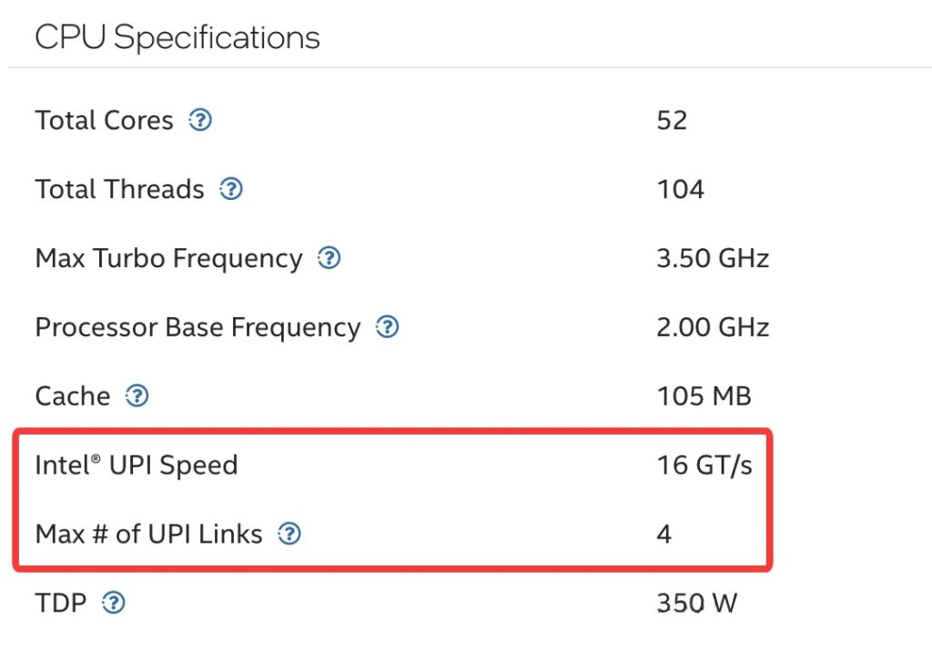
Intel® Xeon® CPU Max 9470 Processor specifications
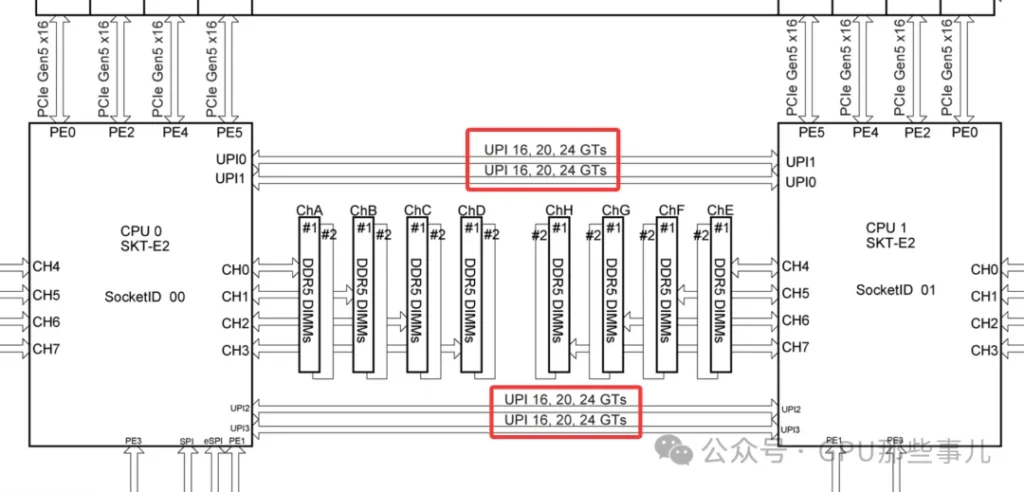
1.1. Intel Platform (Xeon Scalable Series)
- Technology name: Intel Ultra Path Interconnect(UPI)
- Physical form: Each CPU has a dedicated UPI link port. On a dual-socket motherboard, a dense cluster of pins and a corresponding socket are located near the CPU sockets. These are used for installing a UPI interconnect cable or for directly routing the connection through the motherboard PCB layers.
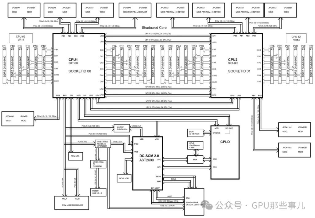
Partial motherboard view of an NVIDIA HGX B300 8-GPU system (Intel platform)
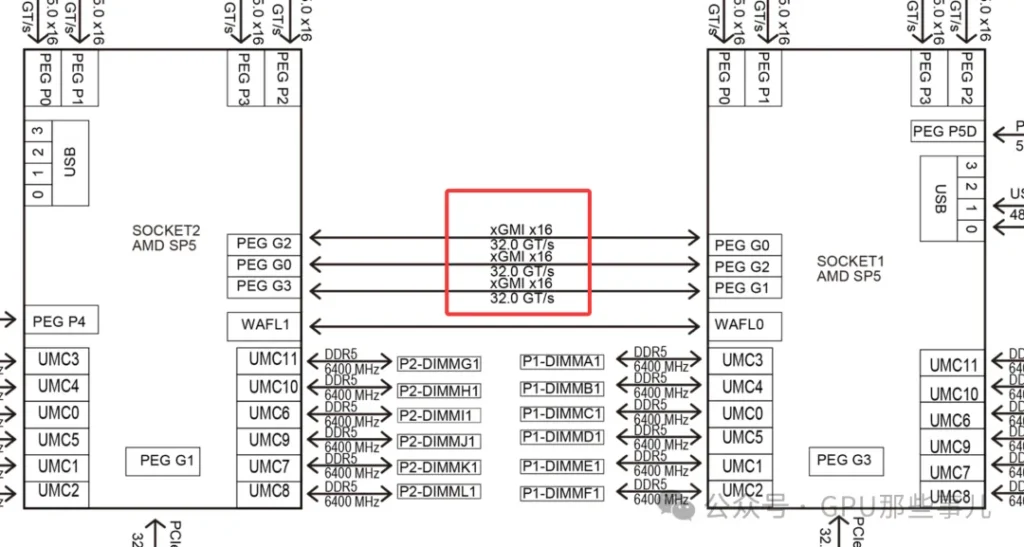
1.2. AMD Platform(EPYC Series)
- Technology name: Infinity Fabric (IF)
- Architecture features: AMD EPYC use an advanced “Chiplet” desing, resulting in a more integrated interconnect.
- Connection metheod: In a dual-socket server, the two EPYC CPUs are directly connected via dedicated Infinity Fabric xGMI links, implemented through dedicated pins and PCB wiring on the motherboard.
某厂Partial motherboard view of an NVIDIA HGX B300 8-GPU AMD system (AMD platform)
Common characteristics: These technologies are ultra-high-speed, low-latency buses specifically designed for CPU-to-CPU communication. They far exceed the PCIe standard of their era in performance and are used to transimit critical data such as cache coherence traffic and memory accesses.
1.3. Resources Consumed by CPU Interconnect
1)No consumption of “user-avaiable” PCIe lanes:
- The PCIe x16 and x8 slot lanes on the motherboard come directly from the CPU. The UPI or IF link between CPUs is an independent physical and logical path, separate from these external PCIe lanes.
- For example, CPU spec sheets often list two numbers, like “64 PCIe lanes+3 UPI links”, 这indicating that the interconnect links are in addition to the lanes (they do not subtract from the 64 lanes available for GPUs, NVMe SSDs, NICs, etc.).
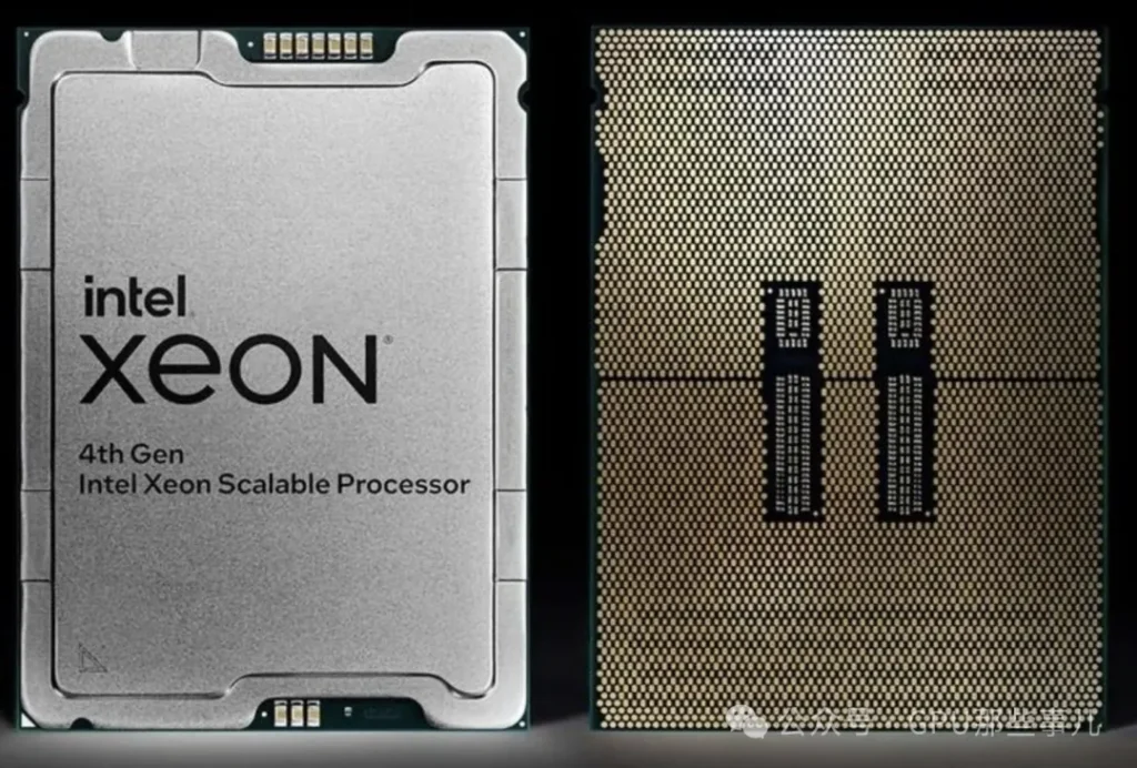
Intel Xeon CPU Max 9480
2)Consumes CPU internal resources and physical pins:
- While the interconnect does not use the user-available PCIe lanes, implementing UPI/IF functionality requires CPU die area, transistors, and package pins. From a system-resource perspective, this is overhead.
- It can be understood that within the CPU there is a “traffic hub” connecting the memory controller, PCIe controller, UPI/IF interconnect module, etc., and the interconnect module has its own dedicated “in/out” port.
2. NUMA Architecture and PCIe Lane “Ownership”
The key challenge in GPU server PCIe lane allocation is ensuring GPUs are “plugged into the right slots” and that software “runs on the right CPU”, to avoid data traveling long distances over the CPU interconnect bus. This is critical for extracting the maximum performance from the system.
2.1. NUMA Architecture
1)Dual-CPU NUMA architecture: After connecting two CPUs, the system forms a NUMA (Non-Uniform Memory Access) architecture. PCIe lane allocation across the system is strictly constrained by this NUMA setup. Key points include:
- Local memory: Each CPU is directly connected to a portion of memory, which can be accessed with the lowest latency.
- Remote memory: A CPU can access the memory attached to the other CPU via the interconnect bus, but with higher latency and lower speed.
- PCIe device affinity: Each PCIe slot is hardwired to a specific CPU. If a GPU is plugged into a slot on CPU0, but the process using it runs on CPU1, then the GPU must access memory (or communicate with the CPU) across the interconnect bus, which degrades performance.
2)When configuring a dual-socket server, it is crucial for optimal performance to place device (GPUs, high-speed NICs, etc.) in appropriate slots and bind processes to the correct CPU. This ensures that most memory and I/O traffic stays local to each CPU.
2.2. PCIe Lane “Ownership”
1)In a dual-CPU system, each CPU’s PCIe lanes are independent and only available locally. This is a key consideration.
2)Resource distribution (for example, suppose each CPU provide 48 PCIe 5.0 lanes):
- CPU 0: Has its own 48 PCIe lanes and its directly attached prtion of memory (local memory).
- CPU 1: Has its own 48 PCIe lanes and its directly attached local memory.
- Interconnect bus: A single high-speed UPI/IF link connects the two CPUs, allowing them to access each other’s memory and devices.
3)GPU Inserts performance differences:
- Scenario A (ideal): Both GPUs are plugged into slots on CPU0. Aprocess running on CPU0 that uses these GPUs will have them access CPU0’s local memory, resulting in the shortest and fastest data path.
- Scenario B (to avoid): One GPU is plugged into CPU0 and the other into CPU1. If a process on CPU0 needs to use GPU on CPU1, the data path is : CPU0 memory -> UPI/IF interconnect -> CPU 1 -> PCIe -> GPU. This adds significant latency and consumes precious interconnect bandwidth, reducing GPU compute efficiency.
2.3. Configuration Recommedations (Golden Rule)
某厂 HGX H200 NVL 服务器主板Motherboard Block Diagram
1)查询主板手册: 在组装或部署GPU服务器前,必须查阅主板手册中的“Motherboard Block Diagram”“Motherboard Layout”。它会明确每个物理插槽连接到哪颗CPU。
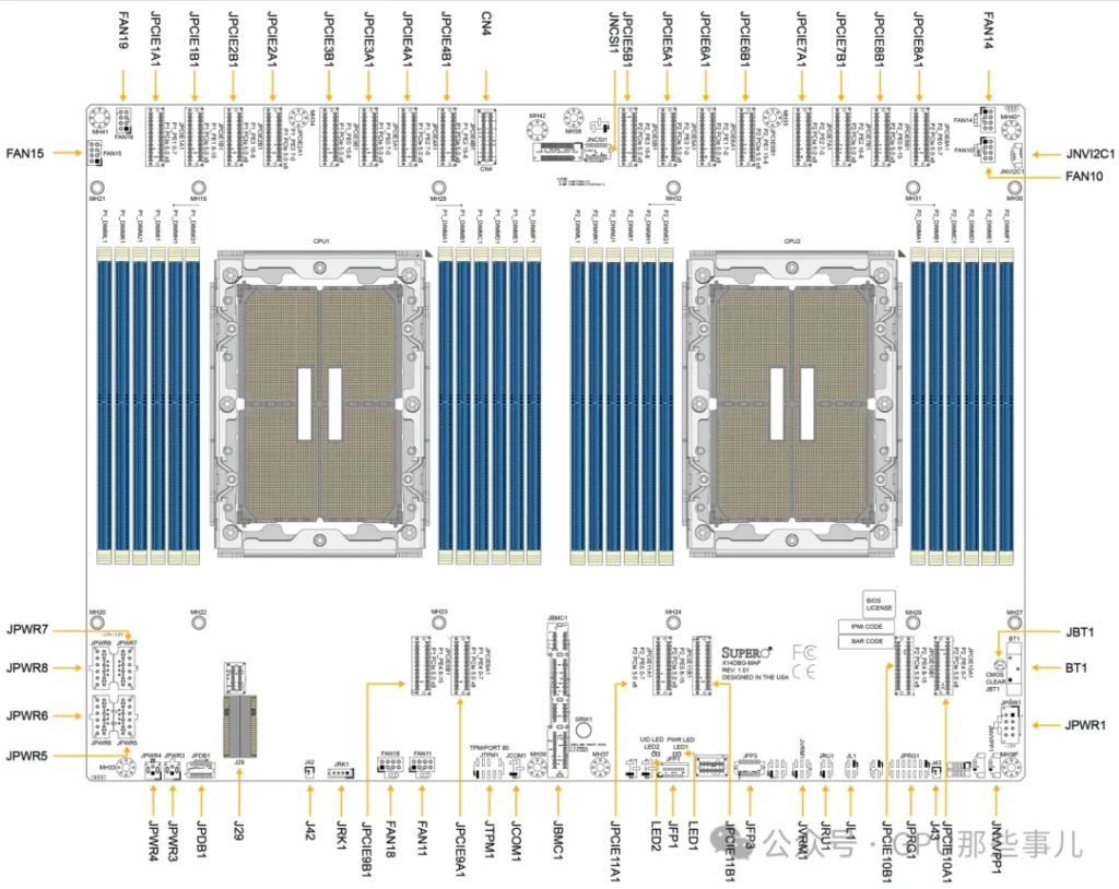
某厂 HGX H200 NVL 服务器主板Motherboard Layout
2)均衡负载与优化路径:
- 如果运行单个需要多GPU并行的任务(如一个大模型训练),尽量将所有GPU安装在同一个CPU所属的插槽上,以确保进程和数据在同一个NUMA节点内。
- 如果运行多个独立的GPU任务,可以均衡地分配到两颗CPU上,但要确保每个任务使用的GPU和内存都尽量位于其运行的CPU本地。
3)使用NUMA感知工具: 在Linux系统中,使用 numactl、lstopo 等工具来查看NUMA拓扑,并在启动任务时绑定CPU和内存节点。
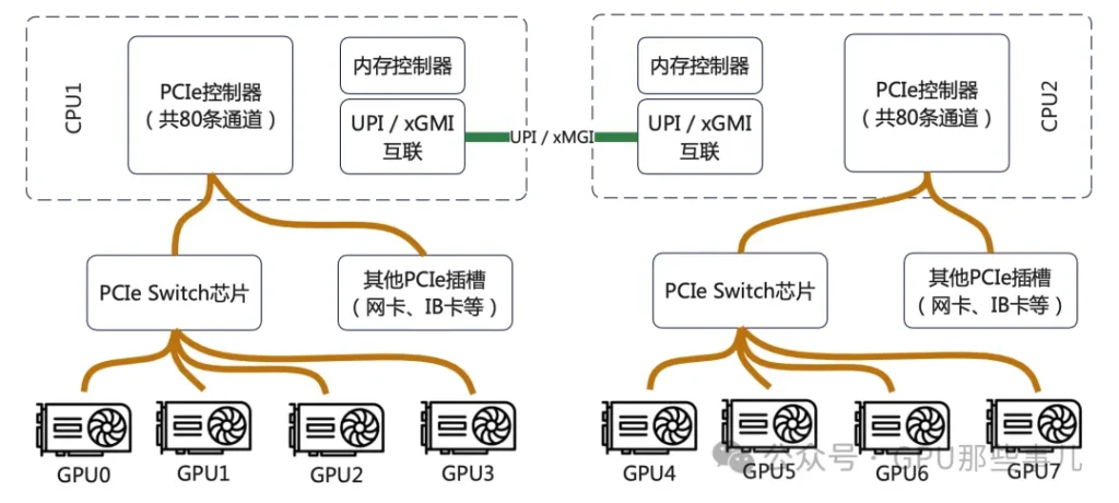
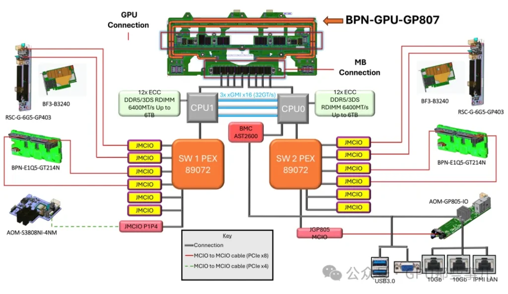
3. PCIe Switch的作用
PCIe Switch并不能增加CPU提供的总物理通道数。它的核心作用是“重新分配和聚合”这些通道,以解决GPU部署中面临的拓扑结构、灵活性和可维护性等关键问题。
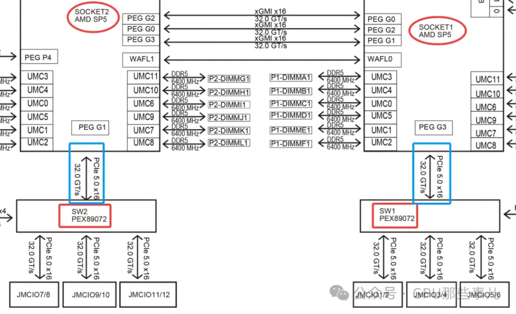
某厂NVIDIA HGX B300 8-GPU AMD平台主板双PCIe Switch(PEX89072)局部图
3.1. 核心作用:打破物理限制,实现最优拓扑连接
1)CPU的PCIe通道是从几个有限的物理接口(如x16)引出的。如果没有Switch:
- 只能把GPU直接插在CPU有限的几个x16插槽上。
- GPU之间如果想高速通信(NVLink/NVSwitch),它们的物理布局将完全受限于主板布线,极其僵化。
2)Switch的作用:它允许将来自CPU的(例如)16条PCIe通道,通过Switch芯片“扩展”成8个x16的物理接口,但这8个接口共享那16条上行通道的带宽。更重要的是,Switch可以智能地配置下游端口之间的连接关系,为GPU之间的NVLink互联提供理想、规整的物理布线基础。HGX主板内部的GPU就是通过这种复杂的PCB布线+Switch逻辑,实现了全互联或部分互联的NVLink拓扑。
3.2. 解决GPU与CPU的比例问题(“对等”与“非对等”访问)
1)在配置8-GPU服务器时,一个根本性难题是:没有单颗CPU能提供足够连接8块GPU的PCIe通道(每块GPU通常需要x16)。
2)Switch的解决方案(以典型8-GPU HGX为例):
- 两颗CPU各自提供一部分PCIe通道(例如每颗提供64条中的48条)给一个或多个PCIe Switch芯片。
- Switch将这些通道聚合后,统一分配给8个GPU物理接口。
- 结果:每块GPU在物理上都连接到Switch,并由Switch决定其上行链路到哪颗CPU。
- 关键优势:通过Switch的配置,可以使任意一块GPU同时访问两颗CPU的内存,或者动态分配带宽。这比将4块GPU固定挂载到CPU0、另外4块固定挂载到CPU1的传统方式要灵活得多,能更好地平衡NUMA架构下的负载。
3.3. 提升可维护性和灵活性(重要!)
1)热插拔支持: PCIe Switch通常提供更好的热插拔支持,这对于需要高可用性的数据中心至关重要。
2)带宽管理和服务质量: Switch可以像网络交换机一样,对下游GPU的PCIe流量进行优先级管理,避免某个GPU的突发流量阻塞其他GPU的通信。
3)故障隔离: 如果某条下游链路或GPU出现问题,Switch可以在一定程度上隔离故障,避免影响整个PCIe树。
在NVIDIA HGX这样的集成式AI服务器中,PCIe Switch是一个至关重要的“赋能”组件。它虽然不能魔术般地变出更多PCIe通道,但它通过一种高效、智能的方式重新分配和路由这些通道,解决了大规模、高密度GPU部署中在拓扑、灵活性、扩展性和管理性方面的根本性挑战,使得8-GPU乃至更复杂的系统能够以最优性能运行。 它的引入,是服务器从“多块独立显卡”向“一体化AI计算单元”演进的关键一步。
4. CPU给PCIe Switch的通道分配原则
在高端GPU服务器(如NVIDIA HGX、DGX及各大OEM的8-GPU机型)中,CPU到PCIe Switch的通道分配是一个经过精心权衡的设计选择,直接影响到系统性能和成本。
4.1. 典型的分配方案(以主流平台为例)
1)当前主流的双路高端GPU服务器通常基于以下配置:
- CPU平台: Intel Xeon Scalable(至强可扩展)或 AMD EPYC
- GPU: 8 x NVIDIA H100/A100/H800等
2)最常见的分配模式是:每颗CPU分配 32 条或 48 条 PCIe 通道给连接GPU的PCIe Switch。
让我们看一个具体的、典型的Intel平台(双路第四代/第五代至强)8-GPU服务器的通道分配图:
如图所示,其核心原则并非追求单GPU带宽最大化,而是确保所有GPU能同时、均衡地访问两颗CPU和全部系统内存,实现聚合带宽最大化。
4.2. 核心分配原则
1)平衡原则(最核心): 确保每块GPU能够以对等(peer-to-peer) 的方式高效访问任意一颗CPU及其本地内存。这是为了优化NUMA性能。如果只从一颗CPU引出所有通道,另一颗CPU下的GPU访问内存将全部成为“远端访问”,延迟大增。因此,通常会让两颗CPU贡献等量的通道给Switch(例如各32条或48条)。
2)“直通”与“交换”分离原则
- 交换路径(Switched Path): 大部分通道(如上述的32/48条)通过PCIe Switch连接GPU,提供灵活拓扑和GPU均衡访问。
- 直连路径(Direct Path): 必须预留一部分CPU通道不经过Switch,直接连接关键I/O设备,如高速网络: 200/400Gb以太网卡、InfiniBand NDR/QDR网卡。这些卡需要低延迟、确定性的x16带宽,直连CPU能获得最佳性能;本地NVMe存储: 用于缓存的超高速SSD;管理/BMC接口。
3)聚合带宽匹配原则: 分配给Switch的总上行带宽(例如双路各48条PCIe 4.0 = 2 x 48 x 2 GB/s ≈ 192 GB/s)需要与GPU对系统内存的聚合访问需求以及网络带宽相匹配。设计时要防止网络成为瓶颈。例如,8块H100通过NVLink同步时,对CPU内存的访问压力巨大,需要足够的上行PCIe带宽来“喂饱”它们。
4)拓扑优化原则: 分配方案需与GPU间互联拓扑(NVLink) 协同设计。在HGX设计中,PCIe Switch的布局和上行带宽分配是为了配合NVLink Switch,让GPU既能通过NVLink高速互访,又能通过均衡的PCIe上行链路与CPU/内存/网络高效通信。
4.3. 不将全部通道都给GPU的原因
某厂NVIDIA HGX B300 8-GPU System Block Diagram
1)这是设计中最重要的权衡点:
- 如果全部通道给GPU: 网络、存储等关键I/O将不得不也连接到Switch的下游,与GPU共享上行带宽,导致网络延迟增加、不确定性增大,这在AI训练和HPC集群中是致命的。
- 如果预留通道过少: 网络带宽可能成为GPU与外界通信的瓶颈,同样限制整体性能。
2)实际方案举例
- NVIDIA DGX H100系统: 采用双路Intel至强CPU。其内部为8块H100 GPU服务的上行PCIe链路总带宽经过精心设计,与CPU内存带宽、NVLink带宽、Quantum-2 InfiniBand网络带宽保持平衡。通常,每颗CPU会贡献大量通道给其内部的Switch fabric。
- 采用AMD EPYC的平台: 由于单颗EPYC CPU提供的PCIe通道数极多(如Genoa高达128条),分配更加灵活。可以实现更复杂的非对称分配,甚至用更少的Switch芯片完成拓扑。
专业GPU服务器中CPU分配给PCIe Switch的通道数不是一个固定值,而是一个系统级设计的结果。其目标是:在GPU、CPU内存、高速网络和存储之间取得最佳的带宽平衡,同时满足GPU对等访问和低延迟通信的需求。典型的双路8-GPU系统中,每颗CPU分配32或48条通道给GPU Switch是经过验证的、能实现整体性能最优的“甜点”方案。