Address
304 North Cardinal St.
Dorchester Center, MA 02124
Work Hours
Monday to Friday: 7AM - 7PM
Weekend: 10AM - 5PM


Powering the Future of Server Infrastructure
Powering the Future of Server Infrastructure
 Byhyperserver
When people talk about DDR Training, they think of DQ, DQS, Write Leveling, Read Gate, and Vref.
But when you actually do DDR5 DIMM bring-up, there is another class of signals that is often underestimated: CA and CS. They do not carry data, yet they decide whether the DRAM can understand the command and whether the correct Rank is selected.
DQ Training solves the questions of whether data can be transmitted and received correctly.
CA Training solves the question of whether the command and address are sampled correctly by the DRAM.
CS Training solves the question of whether this command is really addressed to this Rand or this DRAM.
If compare a DDR system to a conversation, DQ is the return path of the conversation content, CA is the command and address you speak out, and CS_n is whom you call by name to listen. If what you say is not clear, or you call the wrong person, there is no point in training the subsequent read/write data any harder.
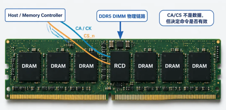
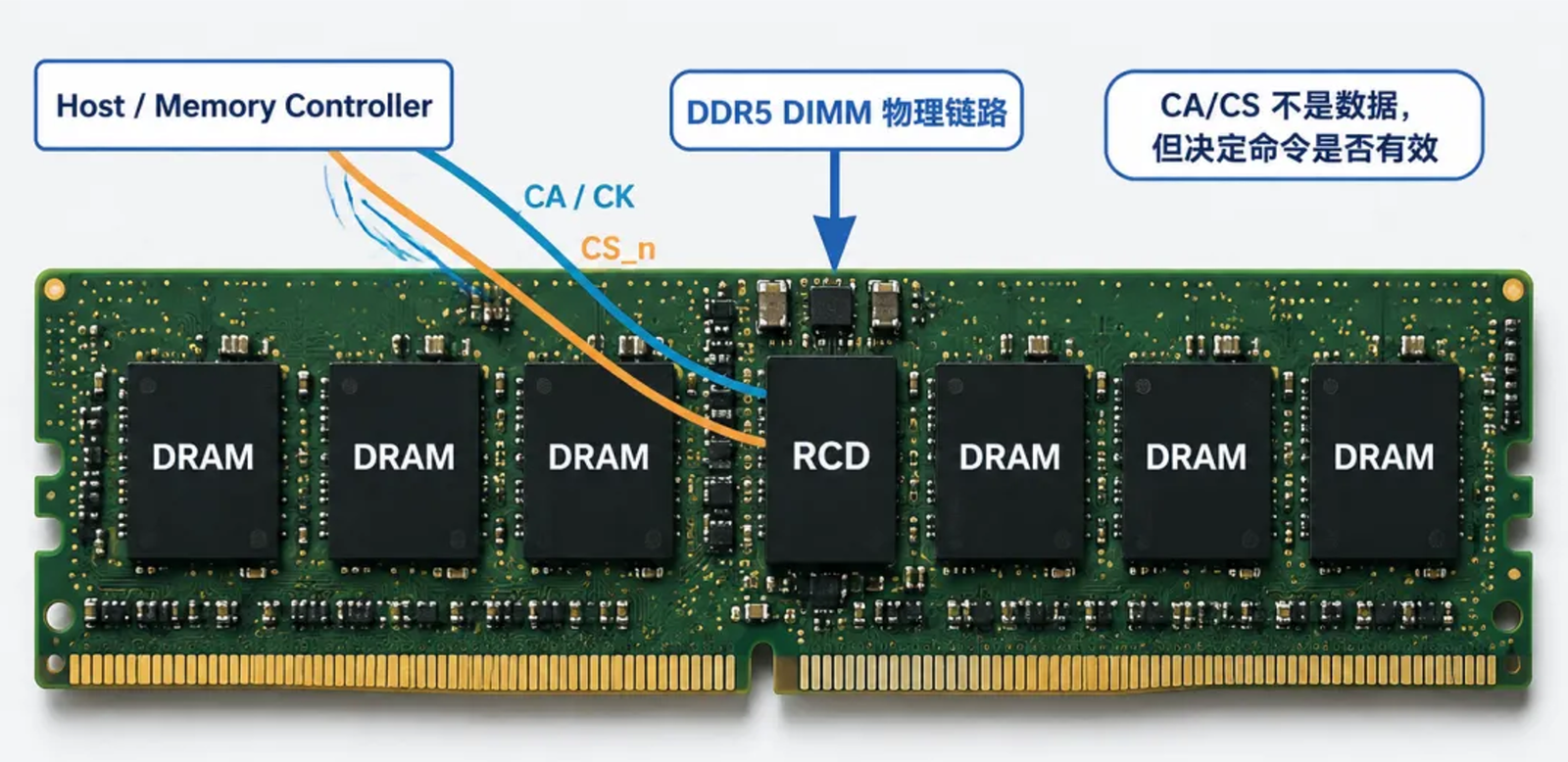
Figure 1: A photo-style schematic. In a DDR5 RDIMM, the CA, CS, and CK issued by the Host usually go into the RCD first and are then distributed by the RCD to the DRAM. UDIMM/SODIMM structures are different, but the core issue is the same: the command/address and chip select must be sampled correctly.
The first impression of Training is “tuning the phase of DQS and DQ”. That is not wrong, because the rad/write data path is the most intuitive: an oscilloscope can show the eye diagram, simulation can sweep out the timing margin, and system training logs also frequently contain keywords such as read gate, write leveling, read DQ, write DQ, and Vref.
But a DDR system does not work just because the data lines look good. A real access always starts with a command and an address: Activate which row? Read which column? Write to which Bank Group? What value is written to the Mode Register?
All of these actions depend on the CA bus and the CS_n chip select signal. If the CA/CS sampling position is wrong, the DRAM may have no idea what you want it to do; or worse, the DRAM may think you sent a different command.
This is also why CA/CS Training deserves more attention from DDR5 onward. In public material, Micron lists CA training and CS training for DDR5 as one of the new capabilities relative to DDR4, whose purpose is to improve the timing margin on the CA and CS pins. In other words, DDR5 does not only raise the data rate; the command/address link itself also increasingly needs engineered calibration.
Do not understand Training as “DDR repairing its own hardware”. The essence of Training is: within the limited window that the hardware already provides, find a more centered sampling point.
CA stands for Command/Address; what the bus carries is command and address information. For example, opening a certain Row, accessing a certain Bank, writing a Mode Register, refresh, precharge, and so on must all be conveyed to the DRAM through CA.
CS_n stands for Chip Select and is active low. It is like a “roll-call signal”: only when CS_n is active does the target DRAM or target Rank consider this command to be addressed to itself; when CS_n is inactive, even if the CA bus changes, the current target should not accept it as a valid command.
DQ is the data bus, and it is responsible for actually moving read/write data. A lot of Training is indeed built around DQ/DQS, because the data eye diagram is extremely sensitive to system stability. But the premise is that the command has first been received correctly and the target Rank has first been selected correctly.
| Object | Engineering meaning | Typical symptom if goes wrong |
| CA | Command/Address bus; tells the DRAM what to do and where to access | Abnormal MRS configuration, access to a wrong address, stuck early in initialization |
| CS_n | Chip select signal; tells which Rank/Device should listen to this command | Target Rank does not repond, the wrong Rank is selected |
| DQ/DQS | Data and data strobe signals; responsible for read/write data sampling | Bit errors, small margin, read/write training failure, unstable stress testing |
The core of CA Training is not “whether the CA lines are connected”, but whether the sampling timing of CA relative to CK is appropriate. The DRAM or RCD does not read CA at any arbitrary time; it samples under its own clock reference. If the CA edge is too close to the sampling point, the setup/hold margin shrinks; if the overall phase of CA is early or late, the command and address may be sampled incorrectly.
In engineering terms, the goal of CA Training is to find a set of CA delay/phase/bit/slip/Vref setting such that, when the DRAM or RCD samples CA, it falls as close as possible to the center of the CA valid window.
Two points need to be emphasized here:
First, the implementation details differ among PHYs, Controllers, DRAMs, and RCDs; register names, training commands, and status feedback methods may all differ.
Second, an article on a public account is not the place to copy one vendor’s manual flow as a “generic DDR standard flow”. A more reliable approach is to explain the engineering logic: enter training mode, send a known pattern, sweep delay, read the feedback, find the pass window, and take the center point.
The core of CS Training is: whether the valid time of CS_n relative to CK and CA is appropriate. CS_n is the chip select; it decides whether the command currently on the CA bus should be accepted by the target object. If CS_n is too early, too late, has an unsuitable pulse width, or has too large a phase offset, then the command may not be received, the wrong object may receive it, or the training status may not be returned correctly.
CS_n looks like just one line, or a few lines, far simpler than a group of CA signals, so many people tend to ignore it. But in read engineering, CS_n failures are often more subtle. Because it is not “one address bit is wrong”, but “was this sentence heard by the target Rank at all”. On multi-Rank DIMMs, CS problems are especially easy to expose: Rank0 may pass while Rank1 training fails; or a certain DIMM model works, but after changing the topology, the DRAM die, or the RCD version, it becomes unstable.
Fix CA and move CS alone: The usual approach in CS Training is first to put CA at a usable or relatively reliable position, and then sweep the delay of CS_n. This is done to separate the variables: if CA and CS move around together, it is hard to tell on failure whether the command content was sampled incorrectly or the chip select timing is wrong.
So you can understand CS Training as: first make sure “what is said is more or less clear”, then adjust “whether the moment of calling the name is exactly right”.
Let the target object sample the CS/CA Pattern: In public material, AMD’s DDR5 CS/CA Calibration describes a similar mechanism: during the training phase, the memory device or the RCD stays in CS or Command Bus Training mode, samples the address and CS pattern, and feeds the sampling status back to the controller. Based on the feedback, the controller adjusts the delay of the CS or CA lines so that they are centered and aligned with CK.
This sentence matters, because it shows that CS/CA Training is not guesswork, nor is it just looking at oscilloscope waveforms. It is a closed-loop process: send a known pattern–> the trained object samples it–> the status returned–> the PHY adjusts the delay–> find the center.
CS is strongly related to Rank: A key point of CS Training is Rank. In a multi-Rank structure, Rank0 and Rank1 may use different CS_n, and go through different topology branches, loads, package paths, RCD output paths, or DIMM routing environments. Even if the CA bus is shared, CS_n may still need per-rank delay settings.
So when analyzing a training failure, do not only ask “is there a problem with the CA lines”; also ask: “Which Rank’s CS failed? Does the failure only happen in a certain DIMM slot? Only at a certain speed bin? Only on cold boot or at high temperature?” These questions get closer to the engineering truth than simply looking at an eye diagram.
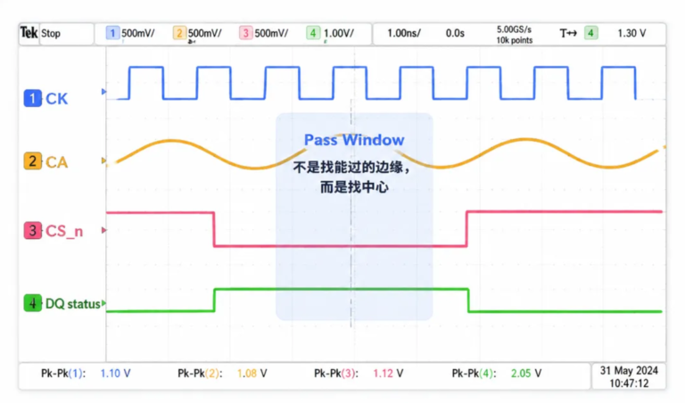
Training goal: center the valid region of CA/CS around the CK sampling point.
Figure 2: A scope-style timing schematic. The intuition of CA/CS Training is simply to move the phase of CA or CS so that the device being trained sees stable valid information near the CK sampling point.
Looking at CA Training and CS Training together, the flows are actually very similar. The difference is that one mainly moves CA and the other mainly moves CS; one focuses on whether the command/address content is sampled correctly, and the other focuses on whether the chip select valid time is correct.
Basic initialization: power, RESET, CK, CKE, ODT, reference voltage, and the necessary mode registers enter the training-enabled state.
Enter training mode: the DRAM or RCD enters CA/CS training mode or the command bus training state.
Send a known Pattern: the Host/PHY sends a training sequence with a known answer on CA/CS.
Sweep Delay: the PHY moves the CA delay or the CS delay, possibly together with parameters such as phase, bit slip, VrefCA, and VrefCS.
Read the feedback: the trained object returns its sampling status, and the controller judges pass/fail at each delay point.
Find the window: record the contiguous pass regions and determine the left boundary, the right boundary, and the window width.
Take the center value: choose the window center or a reliable point near the center, and write it into the PHY registers.
Proceed to subsequent training: once CA/CS is reliable, continue with write leveling, read gate, DQ/DQS centering, Vref, and other training.
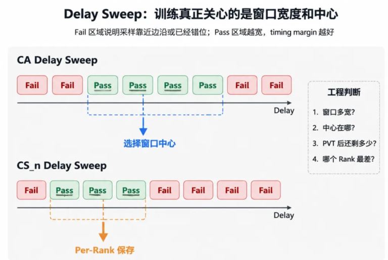
Figure 3: The window view of CA/CS Training. Passing is only the minimum requirement; a wide window, a stable center, and good consistency across Ranks are what engineering really wants to see.
CA and CS are often discussed together because they both belong to the command/address side and are both strongly tied to the sampling relationship with CK. But the problems the two solve are not the same.
| Dimension | CA Training | CS Training |
| Training target | Command/Address | Chip Select, usually CS_n |
| Core question | The command/address is sampled correctly | The target Rank/Device is selected |
| Main adjustments | CA delay, phase, bit slip, possibly together with VrefCA | CS delay, the position of CS relative to CK/CA, possibly together with VrefCS |
| Consequence of failure | The command or address is sampled incorrectly; abnormal MRW/MRR/access behavior | The command is not claimed, or the wrong object claims it |
| Problem scenarios | High speed, long topology, heavy CA load, narrower DRAM input window | Multiple Ranks, RDIMM, slot topology differences, CS branch differences |
| Plain analogy | “Is the content of what is said heard clearly?” | “Was the right person called to listen?” |
In a plain memory-down scenario or some UDIMM/SODIMM cases, the relationship between the Controller/PHY and the DRAM is relatively direct. Although there are still packages, connectors, traces, vias, and topology in between, the command/address link is broadly Host facing DRAM.
With DDR5 RDIMM, things get more complex. Because CA, CS, and CK are usually not distributed directly to all DRAM dies; they first enter the RCD. The role of the RCD is not simply “extending copper”; it buffers the CA bus, chip selects, and clock, and then drives them out to the DRAM. Public RCD product material also clearly lists buffering of the CA bus, chip selects, and clock as one of the core functions.
This means that CA/CS Training on an RDIMM must consider at least two link segments: Host to RCD, and RCD to DRAM. A certain failure point seen in the training log may not only be a motherboard routing problem; it may also be related to RCD configuration, RCD output paths, DIMM layout, Rank organization, and DRAM die loading.
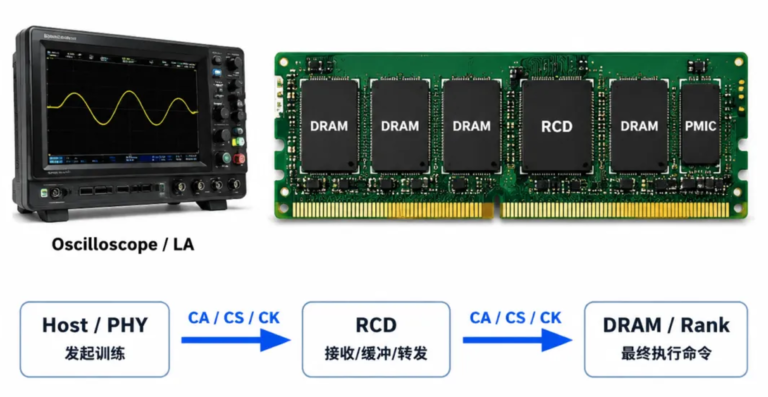
Figure 4: An RDIMM link and lab-style schematic. For an RDIMM, the RCD is not a “transparent copper wire”; the training and debugging of CA/CS/CK must consider the RCD as part of the link.
DQ/DQS problems often show up as bit errors, read/write stress test failures, and small margin on certain byte lanes. CA/CS problems, on the other hand, tend to appear in the first half of initialization, and the symptoms can be rather “mystical”. For example, on the same board, it passes at a reduced frequency but fails at high frequency; with the same BIOS setting, one DIMM passes and another does not; Rand0 passes but RAN1 does not; warm boot works but cold boot is unstable; the oscilloscope shows nothing obviously wrong with DQ, yet the system simply gets stuck in memory training.
At such times, staring only at the DQ eye diagram easily leads your astray. Because the system may not even have reached the real data read/write training stage yet; the earlier CA/cS sampling has already failed.
Common troubleshooting directions
People doing SIPI cannot treat Training as merely a BIOS or PHY matter. Training can adjust delay, but it cannot create a hardware window that does not exist. The board, package, connector, DIMM, RCD, and DRAM input models together determine the actual waveform quality and arrival time of CA/CS.
S-parameters can tell you the insertion loss, return loss, crosstalk, and phase delay of the channel in the frequency domain; IBIS or AMI models help you estimate driver/receiver behavior; time domain simulation lets you see overshoot, ringing, slowed edges, and changes in threshold crossing time; timing analysis tells you how much setup/hold margin is left. What Training ultimately does is find a usable point within these physical limits.
So when analyzing DDR5 CA/CS, I suggest listing at least the following categories of questions:
One sentence that is critical for hardware engineers: Training can help you find the center, but it cannot turn a bad channel into a good channel.
Many people instinctively feel that DQ is the high-speed data line and CA/CS are just control lines, so CA/CS are not that important. This assumption is dangerous on DDR5. Although CA/CS do not carry user data, they determine whether the whole access is valid. Especially at high frequency, with DIMM topology, multiple Ranks, RCD involvement, and a narrower reference voltage window, the margin of CA/CS is not “low-speed” at all.
More practically, when the system cannot boot, you may not even get a chance to see a beautiful DQ eye diagram. Because before that, command/address training, chip select training, Mode Register configuration, and Rank identification may already have failed.
Many people instinctively feel that DQ is the high-speed data line and CA/CS are just control lines, so CA/CS are not that important. This assumption is dangerous on DDR5. Although CA/CS do not carry user data, they determine whether the whole access is valid. Especially at high frequency, with DIMM topology, multiple Ranks, RCD involvement, and a narrower reference voltage window, the margin of CA/CS is not “low-speed” at all.
More practically, when the system cannot boot, you may not even get a chance to see a beautiful DQ eye diagram. Because before that, command/address training, chip select training, Mode Register configuration, and Rank identification may already have failed.
DDR Training does not train DQ alone. DQ/DQS determine whether data can be transmitted and receive stably, but CA/cS determine whether the command can be understood correctly and whether the target object is selected correctly. CA Training solves “is the sentence clear enough”; CS Training solves “did you call the right person”.
From the implementation view, they all follow a similar closed loop: put the DRAM or RCD into the training state, send a known pattern, move the delay or phase, read the sampling feedback, sweep out the pass/fail window, and finally choose the center of the window. This process sounds like a software algorithm, but behind it is real hardware link quality: traces, vias, packages, connectors, DIMM, RCD, DRAM inputs, power noise, reference voltage, ODT, and crosstalk.
So when you encounter a DDR5 DIMM training failure, do not stare only at DQ. First look at which stage the failure occurs in: if it is stuck in early initialization, command bus training, CS/CA calibration, Rank identification, or around MR configuration, then CA/CS must go on the troubleshooting list.
A truly mature DDR debug approach is not to guess by feeling as soon as you see a training fail, but to break the link apart: who is sending? who is receiving? through what feedback? which parameters were swept? how wide is the window? where is the center? which Rank is worst? how much margin is left after frequency, temperature, and voltage change? Once these questions are answered clearly, CA Training and CS Training are not longer mysterious.