Address
304 North Cardinal St.
Dorchester Center, MA 02124
Work Hours
Monday to Friday: 7AM - 7PM
Weekend: 10AM - 5PM

Powering the Future of Server Infrastructure
Powering the Future of Server Infrastructure

Recent SSD markets have entered another round of price increases. Shares of major stroage vendors such as Samsung and SanDisk have repeatedly hit new highs, driven by a deeper imbalance between NAND flash supply and demand and by industry-wide capacity adjustments.
As the ocre storage medium inservers, PCs, and data centers, SSD performance, endurance, and stability directly determine the operating efficiency of the entire IT system. Yet most people still understand SSDs only at a superficial level as “faster than HDDs” and have only a vague grasp of their internal architecture, core technologies such as TFL and wear leveling, and the operating logic of front-end and back-end protocols.
This article breaks down the complete operating principles of SSDs from the hardware architecture (controller, NAND chips, cache) to the software architecture (FTL core, firmware), and from front-end protocols (SATA, NVMe) to back-end flash control, with special focus on the core mechanisms in FTL such as wear leveling and garbage collection.
Before breaking down the architecture and principles, first establish a core understanding: the essential difference between SSDs and traditional hard disk drives (HHDs) is not whether they have mechanical parts, but the fundamental difference in storage media and data read/write mechanisms. This is the core reason SSDs are faster, consume less power, and are more shock-resistant, and it is also the foundation for understanding the architecture and principles that follow.
HDDs read and write data by rotating heads and addressing platters; the physical nature of mechanical motion results in high latency (millisecond level) and poor random read/write performance.
SSDs, by contrast, are based on NAND flash chips (a non-volatile storage medium) and perform reads and writes through electronic signals control charge storage. There is no mechanical motion, so latency can be as low as microseconds, and random read/write performance is 10-100 times that of HDDs.
However, behind SSD’s advantages are inherent limitations: they physical characteristics of NAND flash (must be erased before writing, finite program/erase cycles) mean it must reply on a complex software layer (FTL, Flash Translation Layer) and hardware control to become “as easy to use as an HDD”. This is the core challenge in SSD architecture desing – and it is the key topic we will now break down.
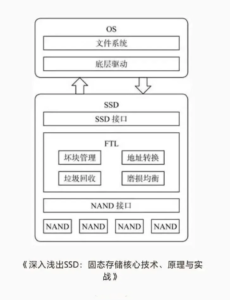
The SSD architecture is essentially a collaborative system of “hardware+software” , divided into hardware architecture (responsible for physical data storage and signal transmission) and software architecture (responsible for logical data management and feature adaptation). Together, they solve NAND’s physical limitations and enable efficient, reliable storage services.
The overall architecture can be divided into three layers, from outside to inside: the fron-end protocol layer (interacting with the host) -> the core control layer (hardware controller+software FTL) -> the back-end flash layer (NAND flash chips), plus auxiliary cache and firmware modules, forming a complete SSD system.
The core of the SSD hardware architecture is “controller+NAND flash+cache”, plus auxiliary components such as the interface and power circuitry. This is the SSD’s “body” – all software logic (such as FTL) must ultimately be implemented through hardware components.
The controller chip is the core of the SSD, equivalent to a CPU. It coordinates all data reads and writes, scheduling, error correction, and communication with the hosts. Its performance directly determines SSD read/write speed, latency, endurance, and stability.
Core functions include: parsing front-end protocols (SATA/NVMe, etc) and receiving host read/write requests (such as LBA logical address requests); executing FTL algorithms (logical-to-physical address translation, wear leveling, garbage collection, etc); scheduling NAND flash read/write/erase operations to enable multi-channel and multi-chip parallel operation (improving throughput); performing error correction (ECC) to repair bit errors that occur during NAND reads and writes and ensure data integrity; and managing cache (DRAM/HBM) to support temporary storage and acceleraton while reducing pressure on NAND flash reads and writes.
Mainstream controller vendors include Samsung (Elpis), Phison (PS5021), Silicon Motion (SM2269XT), and Marvell. The algorithm optimization of different controllers – especially FTL – is a major reason for SSD performance differences. This is one of the key reasons Samsung SSDs command a premium and are know for strong stability.
NAND flash chips are the core medium by which SSDs store data, equivalent to a warehouse. Their type, process, and layer count directly determine SSD capacity, endurance, speed, and cost – and are also the key cause of the recent SSD price increases (NAND capacity contraction and rising demand).
First, the core physical characteristics of NAND flash must be clear, because they are essential to understanding FTL: non-volatility-data is not lost when power is removed, so no continuous power is required (unlike DRAM cache); inconsistent read/write/erase granularity – the smallest read/write unit is a page (typically 4KB, 8KB or 16KB), while the smallest erase unit is a block (a block contains tens of pages, e.g. 64 pages); no in-place overwrite – NAND cannot directly overwrite existing data and must erase and entire block before writing new data (this is the fundamental reason FTL exists); and finite endurance- each block has a limited number of program/erase cycles (SLC can reach 100,000+, TLC is about 1,000-3,000, QLC about 300-1,000), after which the block fails and can no longer store data.
The NAND hierarchy, from large to small, is : Package -> Die -> Plane -> Block -> Page. The controller uses multi-channel parallel control of multiple dies/planes to parallelze data reads and writes and increase SSD throughput. For example, mainstream SSDs support 8 or 16 channels and can read and write multiple chips simultaneously, doubling speed.
Mainstream NAND type comparison (key selection factor for enterprise and consumer use).
Type | Bits per Cell | P/E Cycle Endurance | Speed | Cost | Typical Use |
SLC | 1 bit | 100,000+ | Fastest | Highest | Enterprise core workloads, military applications, high-end servers |
MLC | 2 bits | 3,000–10,000 | Medium-high | Medium-high | General enterprise workloads, high-end consumer SSDs |
TLC | 3 bits | 1,000–3,000 | Medium | Medium | Mainstream consumer SSDs, non-core enterprise workloads |
QLC | 4 bits | 300–1,000 | Medium-low | Lowest | Entry-level consumer SSDs, large-capacity storage such as surveillance and backup |
A note: the main recent price increase is driven by TLC and QLC chips, which are the mainstream types in both consumer and enterprise markets. As core chip manufacture, Samsung and SanDisk have reduced capacity, widening the supply-demand gap, which directly pushed up SSD end-user prices and lifted stock prices.
The core role of the cache module is to temporarily store frequently accessed data and buffer read/write requests, reducing the number of direct NAND accesses and thereby lowering latency and improving performance. It functions like the SSD’s “temporary warehouse”, prioritizing high-frequency data and avoiding “using a sledgehammer to crack a nut”.
Mainstream cache types include: DRAM cache, and independent DRAM chip (such as DDR4/DDR5). The larger the capacity, the better the cache effect, making it suitable for high-frequency read/write scenarios such as servers and design workstations. Its drawbacks are higher cost and the fact that cached data is lost when power is removed (so it must be paired with power-loss protection circuitry). HMB (Host Memory Buffer) has no dedicated DRAM; it borrows host memory (such as a PC’s RAM) as cache, which lower cost and suit entry-level consumer SSDs. Its downside is dependence on host memory and slightly weaker performance than independent DRAM cache.
The core logic is : when the host writes data, it first goes into cache; once the cache is full, data is written in batches to NAND flash (reducing frequent NAND writes and lowering latency). When the host reads data, it first searches the cache; if not found, it reads from NAND, improving read speed.
The interface is responsible for connecting to the host and transmitting data and commands. Mainstream interfaces are SATA and PCIe (NVMe protocol); the interface type directly determines the maximum SSD bandwidth, which will be discussed in detail in the front-end protocol section below. The power circuitry supplies stable voltage to the controller, NAND, and cache to prevent data loss cause by voltage fluctuations.
Power-loss protection (PLP) is essential in enterprise SSDs: when power is lost, capacitors or supercapacitors provide power long enough for the data in cache to be written into NAND flash, preventing data loss. This is one of the key differences between enterprise SSDs and consumer SSDs.
FTL’s core role is “translation+management”: on one hand, it translates host-sent logical addresses (LBA, Logical Block Address) into NAND flash physical addresses (PBA, physical Block Address), acting as a translator,; on the other hand, it manages NAND space and endurance, solving the problems of non-overwrite writes and finite erase endurance, acting as a manager. Put simply: the host does not know NAND’s physical structure (pages and blocks); it only knows logical addresses (for example, LBA 100). FTL maps that logical address to a specific NAND page (for example, Die 1, Plane 2, Block 5, Page 8) and manages the read, write, and erase behavior of that page to ensure data safety and maximize lifespan.
FTL has three core functions that are essential to understand, especially for enterprise operations: address mapping, wear leveling, and garbage collection. These three are interrelated and all are necessary.
(1) Address Mapping: the core “translation” from logical address to physical address
This is the most basic function of FTL and the prerequisite for solving the overwrite problem. Since NAND cannot be overwritten in place, new data can only be written to a free page, while the host recognizes only fixed logical addresses. FTL therefore maintains a “mapping table” that records the physical address corresponding to each logical address.
Mainstream mapping schemes include three types, each with pros and cons:
Page Mapping, the finest-grained scheme, in which each logical page (LBA) corresponds to one physical page (PBA). It has the highest space utilization and best performance, but the mapping table is large (for example, a 1TB SSD may require about 128MB of mapping table), so DRAM cache is needed to store it, increasing cost. This is used in high-performance enterprise SSDs and high-end consumer SSDs.
Block Mapping maps in block units, where one logical block corresponds to one physical block. The mapping table is small, does not require much DRAM cache, and is low-cost, but space utilization is lower, wear leveling is weaker, and performance is only average. It is used only in entry-level consumer SSDs and low-capacity SSDs.
Hybrid Mapping combines page-level and block-level mapping advantages: “hot data” that is accessed frequently uses page mapping for performance, while “cold data” that is accessed infrequently uses block mapping to save space. This balances performance and cost and is common in mid-range consumer SSDs.
FTL maintains the mapping table in real time. When data is overwritten or deleted, the old physical page is not erased immediately. Instead, it is marked as invalid, while new data is written to a new free physical page and the mapping table is updated so the logical address points to the new physical page. This is also the prerequistie for garbage collection.
(2) Wear Leveling: the core algorithm for extending SSD lifespan
As noted above, each NAND block has a fixed erase endurance (P/E cycle). If certain blocks are erased and written frequently (fox example, log data that is written often), they will fail early, causing the SSD’s usable capactiy to shrink or even the drive to fail. The core purpose of wear leveling is to make the erase count of all blocks as unifrom as possible, thereby maximizing the SSD’s overall lifespan.
Wear leveling has two types, both enabled simultaneously by FTL and working together:
Dynamic Wear Leveling targets “hot data” (frequently written or overwritten data). FTL preferentially writes such data to blocks with lower erase counts, avoiding overuse of some blocks. For example, if one block has only 100 erase cycles while others have 1,000, FTL will prioritize the low-wear block for high-frequency writes to balance wear.
Static Wear Leveling targets “clod data” (data that has not been modified or deleted for a long time). Such data sits on blocks with low erase counts, while other blocks may be close to their endurance limit.
FTL periodically migrates cold data from low-wear blocks to high-wera blocks, then erases the low-wear blocks so they become free blocks for hot data. This prevents cold data from occupying “young” blocks for too long, which would otherwise leave young blocks idle and cause older blocks to fail early.
A supplemental note: over-provisioning is an important aid to wear levling. SSD vendors reserve a portion of capacity (typically 5%-20%) that is not exposed to the user and is used for wear leveling, garbage collection, and bad block replacement. The more reserved capacity, the better the wear leveling effect and the longer the SSD lifespan. Enterprise SSDs usually reserve 10%-20%, while consumer SSDs reserve 5%-10%.
(3) Garbage Collection (GC): the “cleanup tool” that frees invalid space
Because NAND cannot be overwritten in place, after new data is written to a new page, the lod page is marked invalid (but it still occupies physical space). Over time, invalid pages accumulate, reducing free space and degrading performance.
Garbage collection’s core function is to reclaim the space occupied by invalid pages so it can be used again for new data. The full garbage collection flow is essential to understand SSD performance fluctuations: Identification – FTL scans all NAND blocks in real time and identifies blocks containing invalid pages (for example, a blcok with 10 pages where 6 are invalid and 4 are valid). Migration – all valid pages from that block are copied to a free block.
Erasure – all invalid pages and the valid pages that have already been migrated are erased from the original block, making it a free block available for new data.
Update – the mapping talbe is updated so that the logical addresses of the original valid pages point to the newly migrated physical pages.
Important: garbage collection runs automatically in the background. When SSD free space falls below a threshold (for example, 20%), FTL automatically triggers garbage collection. At that moment, SSD read/write performance mayy temporarily drop because the controller must handle both host I/O and garbage collection at the same time.
This is normal and is one of the main reasons SSD performance fluctuates. Best practice in enterprise environments is to avoid keeping SSDs at very high utilization for long periods (recommend below 80%), otherwise garbage collection will triggered frequently, reducing performance and shortening lifespan. At the same time, enable the TRIM command (discussed below) so the host can promptly notify the SSD which data is invalid, improving garbage collection efficiency.
Firmware is the software program embedded in the SSD controller, equivalent to the SSD’s operating system. All FTL algorithms – address mapping, wear leveling, and garbage collection – are executed through firmware.
The degreee of firmware optimization directly affects SSD performance, staility, and lifespan. Core functions include running FTL algorithms to manage NAND space and endurance; parsing front-end protocols and communicating with the host driver to receive and respond to host read/write requests; performing ECC to repair NAND bit errors; managing cahce for temporary storage and acceleration; and monitoring SSD operating conditions such as temperature, wear level, and bad block count, then reporting these to the host.
Firmware can be upgraded to improve performance, fix bugs, and enhance stability. In enterprise SSD operations, periodic firmware upgrades are an important maintenance task, but they carry risk and data should be backed p in advance.
Drivers are installed on the host (PC or server) and handle communication between the host and the SSD. They translate host read/write requests (such as file I/O) into protocol comands that the SSD can recognize (such as SATA/NVMe commands), while also feeding SSD status information (such as capacity, temperature, and wear) back to the host. Mainstream driver types include SATA SSD, which typically use generic drivers built into Windows and Linux and do not require separate installation, and NVMe SSDs, some of which require dedicated rivers (such as Samsung NVMe drivers) to achieve optimal performance, especially enterprise NVMe SSDs where vendor drivers can optimize latency and improve throughput.
After covering hardware and software architecture, we now break down the SSD’s “input/output channels”: the front-end protocol, which communicates with the host, and back-end control, which communicates with NAND flash. These two parts directly determine SSD transfer speed, compatibility, and expandability, and are key criteria for enterprise selection.
The front-end protocol is the communication standard between the SSD and the host. It defines data transfer format, command, and bandwidth. Mainstream protocols are SATA and NVMe, and their differences are significant – they directly determine the performance ceiling of an SSD and are one of the key disinctions between consumer SSDs and enterprise SSDs.
SATA (Serial ATA) is the traditional storage protocol, originally designed for HDDs and later adpter for SSDs. It includes SATA1.0(1.5Gbps), SATA2.0 (3Gbps), and SATA3.0 (6Gbps).
The current mainstream version is SATA3.0, with a maximum bandwidth of about 600MB/s (actual transfer speeed about 500-550 MB/s). Its core characteristics are: extremely strong compatibility, supporting all devices with SATA interfaces (PCs, servers, laptops) and allowing direct replacement of HDDs without hardware of software changes; low performance ceiling, because protocol bandwidth limits sequential read/write speed to about 550MB/s and random read/write speed to about 100-200MB/s, making it unsuitable for enterprise high-frequency write/read workloads such as databases and virtulization; and low cost, because SATA SSD controllers and interfaces are inexpensive, making them suitable for entry-level comsumer use and large-capacity backup scenarios.
NVMe (Non-Volatile Memory Express) is a protocol designed specifically for SSDs. It is based on PCIe and avoids SATA’s performance limits.
Current mainstream vesions are NVMe 1.4 and NVMe 2.0, and maximum transfer bandwidth depends on the PCIe version (PCIe3.0 x4 about 32Gbps, PCIe4.0 x4 about 64Gbps, PCIe5.0 x4 about 128Gbps). Its core characteristics, especially important for enterprise use, are: extremely high performance, with sequential read/write speeds of 3,000-10,000MB/s and random read/write speeds of 1,000k-2,000k IOPS, 5-10 times that of SATA SSDs, making it suitable for high-frequency, low-latency workloads such as databases, virtualization, and AI training; very low latency, because NVMe simplifies the data transfer path and can reduce latency to 10-50 microseconds, far lower than SATA SSDs (100-200 microseconds); support for multiple queues, allowing concurrent processing of many read/write requests (for example, 64K queue depth), improving multi-task performance; and higher cost, becuase NVMe SSD controllers and interfaces are more expensive, with prices typically 1.5-2 times those of same-capacity SATA SSDs, making them suitable for enterprise core workloads.
A note:NVMe is further divided into NVMe over PCIe (local use) and NVMe over Fabrics (NVMe-oF, remote use). The latter is used in data centers for remote SSD sharing and high-speed access, similar in logic to NFS sharing but with much higher performance.
TRIM is a “cooperative command” between the host and the SSD. Its core purpose is to notify the SSD which data is invalid. When the host deletes a file, it does not directly delete physical data from the SSD; instead, it uses the TRIM command to tell the SSD that the data corresponding to a logical address is now invalid. FTL then marks the corresponding physical page as invalid and prepares it for garbage collection.
The core value is that after TRIM is enabled, SSD garbage collection efficiency improves significantly, because less data needs to be migrated during cleanup, reducing performance fluctuations while also extending SSD lifespand. Enterprise SSDs should enable TRIM (supported by both Windows and Linux).
Back-end control is the communication mechanism between the controller and NAND flash. It converts FTL commands (read, write, erase) into electrical signals that NAND flash can understand, while also implementing parallel control across multiple channels and chips to improve data transfer efficiency – essentially the SSD’s internal bus.
Core components and logic include: the flash controller (integrated in the controller), which drives NAND flash chips to perform read/write/erase operations and supports NAND interface standards such as ONFI and Toggle (mainstream is ONFI 4.0); multi-channel parallelism, where the controller uses multiple channels (such as 8 or 16 channels) to control multiple NAND chips simultaneously, with each channel connecting to multiple dies to enable parallel reads and writes – this is the core means by which SSD throughput is increased (for example, an 8-channel SSD can read and write eight chips simultaneously, making it eight times the speed of a single-channel design); and bad block management, where the back-end control continuously detects NAND blocks, marks failed bad blocks as unusable to prevent data loss, and uses reserved over-provisioned space to replace them, ensuring normal SSD operation.
The degree of back-end parallelism (number of channels and chips) directly determines maximum SSD throughput. Enterprise high-performance SSDs usually adopt 16-channel or 32-channel designs; the higher the parallelism, the stronger the performance.
Form factor is the SSD’s physical size and determines where the SSD can be installled (PCs, servers, laptops). Different scenarios require different form factors, which is also an important selection factor in enterprise environments. Common SSD form factors can be divided into four types, with the first three being the most important.
Size: 100mm (L) x 70mm (W) x 7mm /9.5mm (H), the same as traditional 2.5-inch HDDs, making it the most universal form factor. The interface is primarily SATA (with a few U.2 versions supporting NVMe), and it can directly replace an HDD without hardware modification. Typical use cases: consumer PCs, laptops, servers (non-high-density deployments), and large-capacity backup storage. Its compatibility is extremely strong, and it is one of the most mainstream form factors today.
The M.2 form factor is miniaturized, with common sizes 2230 (22mmx30mm), 2242 (22mmx43mm), 2260 (22mmx60mm), and 2280 (22mmx80mm), of which 2280 is the most mainstream. Interfaces are divided into STA (B key) and NVMe (M key), and the NVMe-based M.2 SSD (M key) delivers best performance, making it the preferred choice for enterprise servers and high-end PCs. Use cases include enterprise servers (high-density deployments), high-end PCs, and laptops (thin-and-light systems). Its small size saves chassis space and suits high-density deployments such as data center blade servers.
Size is the same as a 2.5-inch SSD (100mmx70mmx7mm), but the interface differs: it uses the U.2 interface (SFF-8639) and supports NVMe only. Core characteristics include strong performance (supporting PCIe 4.0/5.0) and high reliability (supporting hot swap and power-loss protection), making it suitable for enterprise core workloads. Typical uses include enterprise servers and core data-center storage such as databases and virtualization. Hot-swap makes maintenance easier, and power-loss protection safeguards data. It is the preferred form factor for high-performance enterprise SSDs.
mSATA SSDs are miniaturized and mainly used in older laptops and embedded devices, but they are gradually being replaced by M.2 SSDs. U.3 SSDs are the upgraded version of U.2, supporting PCIe5.0 and higher bandwidth, making them suitable for next-generation high-performance storage in data centers.
Combining the architecture, protocols, and FTL core discussed above, we can trace a complete “host writes data” workflow to connect all concepts and fully understand how SSDs work (the read flow is similar, just in reverse): the host initiates a wirte request.
The host (for example, a server) converts the file-system write request into a logical address (LBA) and sends it to the SSD controller through the front-end protocol (SATA/NVMe); the controller receives and parses the request. It parses the front-end protocol command, extracts the logical address (LBA) and data, and temporarily writes the data into cache (DRAM/HMB), decoupling speed; FTL address mapping.
FTL queries the mapping table and assigns a free phsical address (PBA, corresponding to a page in NAND flash) to the current logical address (LBA), while updating the mapping table; back-end control performs the wirte. The controller uses back-end control (multi-channel) to write the data from cache into the corresponding physical page in NAND flash (at this point the new data is written, while the page corresponding to the old data is marked invalid); FTL maintenance and optimization. If the current block has already undergone many erase cycles, FTL uses wear leveling to write subsequent data to blocks with fewer erase cycles.
When free space falls below a threshold, FTL auto matically triggers garbage collection to reclaim the space occupied by invalid pages; and the controller returns the result. The controller send a successful-write signal back to the host through the front-end protocol, and the write process is complete.
The operating principle of an SSD is fundamentally a collaboration between hardware and software. Its core is to use FTL to solve NAND flash’s physical limitations, use front-end protocols to communicate at high speed with the host, and use back-end control to perform parallel read/write operation on NAND flash. Although it seems complex, it can be broken down into three main parts: hardware (controller, NAND, cache), software (FTL, firmware), and protocols (front-end SATA/NVMe, back-end ONFI).