Interpretation of DDR Training During SSD Power-Up
1. Role of DRAM in SSD
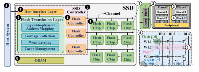
A common SSD architecture is illustrated by the diagram below: it show the SSD controller, DRAM, NAND chips, and how the flash controller interacts wit NAND architecture. It also briefly explians hierarchical NAND concepts such as die, plane, block, page, and cell. This figure represents the classic SSD architecture.
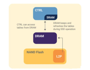
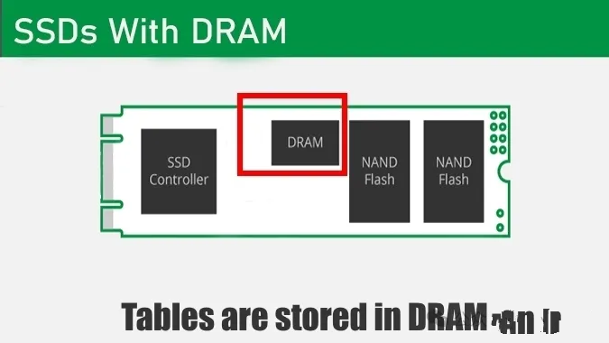
Modren solid-state drives (SSDs) commonly include a certain amount of DRAM as a cache. Its primary function is to store the FTL (Flash Translation Layer) mapping table and other temporary data, accelerating the SSD’s data processing efficiency.
The relationship between DRAM cahce capacity and NAND flash capacity is not fixed, but generally, larger-capacity SSDs require larger DRAM to maintain efficient FTL management. Reasons include:
Mapping complexity increases. As NAND capacity grows, the FTL mapping table becomes larger and more pages/blocks require management, necessitating additional cache space for these mappings.
Pefromance requirements. Large SSDs often target high-performance applications; higher read/write rates demand quicker cache responses. Sufficient DRAM ensures that under high concurrent workloads the FTL tables need not be repeatedly reloaded, avoiding performance bottlenecks.
Cost vs. value. Although DRAM cost is significant, vendors provision DRAM according to product positioning. Histrical heuristics (for example, 1MB DRAM per 1GB NAND) are not strict rules; different SKUs may adopt different ratios.
In traditional SSDs, DRAM plays essential roles such as storing metadata, buffering write data, coalescing small writes into larger ones, and assisting internal data movement for garbage collection. Because NAND behaves differently from spinning media, DRAM helps bridge these differences and optimize overall throughput.
2. Why DDR Training is Required at SSD Power-up
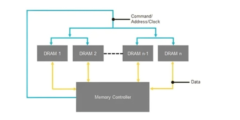
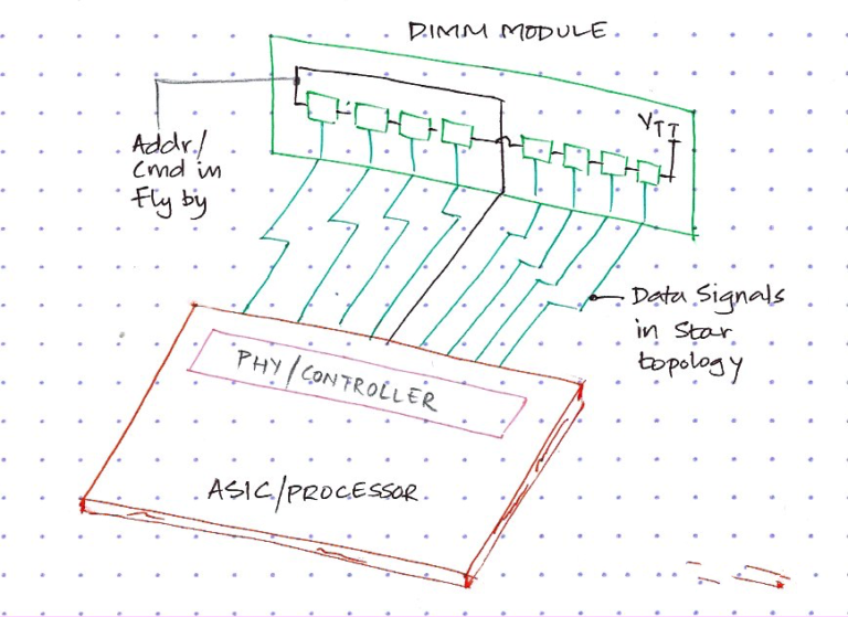
SSD DRAM typically operates at high data rates (e.g., DDR4 1600-3200Mbps or higher) and commonly uses a JEDEC-defined fly-by topology (clock/command lines daisy-chained across multiple DRAM devices). After power-up, theree core problems must be resolved by training:
2.1 Electrical characteristic deviations caused by PVT (Process, Voltage, Temperature) variations
Drive strength and on-die termination (ODT) of DDR are significantly affected by process, supply voltage, and temperature. Examples:
- Process variation: the nominal 240Ω pull-up resistor on DRAM may vary by ±10% across parts in the same batch.
- Voltage ripple: during SSD power-up, VDDQ (the DDR data supply) can exhibit ±5% ripple.
- Temperature drift: as operating temperature rise from 0°C~85°C, DRAM output impedance may change by more than 15%.
If left uncalibrated, these deviations cause increased signal reflections and crosstalk and can lead to data transmission errors.
2.2 Timing Skew introduced by fly-by topology
SSD DDR channels are routed in a fly-by fashion (CK, command/address lines daisy-chained across DRAM devices) rather than point-to-point. This causes:
- Clock (CK) arrival time differences across DRAM devices up to 1-2ns (equivalent to 2-4 UI at DDR4-3200).
- DQS and DQ path length differences that shrink the timing alignment window.
Example: when the SSD controller issues a WRITE, the column address (CA) and DQ must meet the CAS write latency (CWL) timing constraint (e.g., CWL=9). If skew causes DQ to arrive at the DRAM outside the CWL window, write failures can occur.
2.3 Signal integrity degradation in dynamic environments
During SSD operation, NAND reads/writes and controller background tasks can:
- Couple power noise into DDR channels.
- Cause PCB trace impedance shifts due to temperature changes.
- And, over long-term use, DRAM die aging can reduce output signal amplitude.
Training dynamically adjusts sampling windows and reference voltages to maintain the data-eye margin (typically targeting horizontal/vertical margin ≥20% UI).
Definition: DDR training is the controller (or DDR PHY) algorithmic process that adjusts timing, voltages, and impedance parameters so the DDR link meets JEDEC timing specifications (such as tDQSS, tSETUP, tHOLD). Core objectives include:
- Aligning CK, DQS and DQ timing relationships;
- Optimizing VrefDQ to ensure robust ‘0’/’1′ decision thresholds;
- Calibrating drive strength and ODT to suppress reflections;
- Maximizing the data eye area and minimizing bit error rate (BER ≤ 1×10⁻¹²).
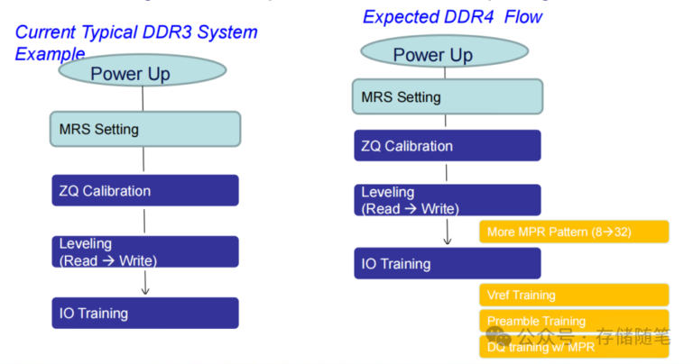
Per JEDEC (e.g., JESD79-4 for DDR4 and JESD209-5 for LPDDR5), DDR training at SSD power-up typically follows four tightly coupled stage; each stage is required.
3. DDR Training Procedure During SSD Power-up
After covering hardware and software architecture, we now break down the SSD’s “input/output channels”: the front-end protocol, which communicates with the host, and back-end control, which communicates with NAND flash. These two parts directly determine SSD transfer speed, compatibility, and expandability, and are key criteria for enterprise selection.
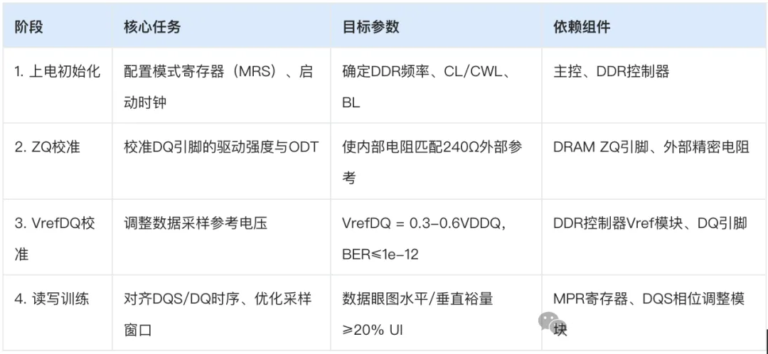
3.1 Phase 1 – Power-Up Initialization
Goal: transition DRAM from RESET to IDLE and configure baseline operating parameters.
Power & Reset Sequence:
- After SSD power-up, apply VDD (core) and VDDQ (data) to DRAM and wait for rails to stabilize (commonly ~100 us).
- Release RESET_n and assert clock enable (CKE).
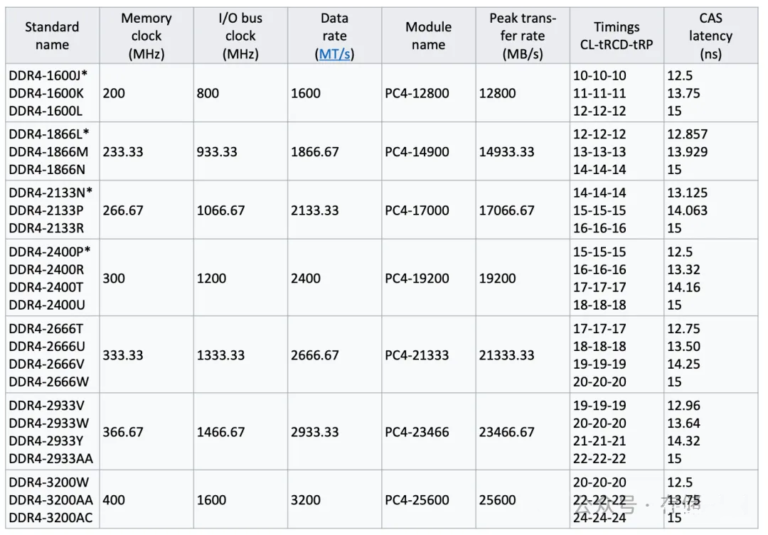
- Start the differential clock (CK_t/CK_c) at a low rate (e.g., 200MHz), then step to the target frequency (e.g., 1600MHz for DDR-3200).
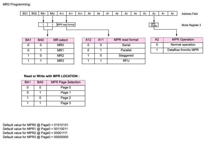
Mode register setup (MRS commands) Controller programs DRAM mode registers in JEDEC order (MR0->MR1->MR2_>…). Typical settings:
- MR0: CAS latency (CL), burst length (BL, typically 8), self-refresh modes.
- MR1: Drive strength (e.g., DS=RZQ/4), ODT setting (e.g., RTT_NOM=240Ω).
- MR2: CAS write latency (CWL), dynamic ODT (RTT_WR).
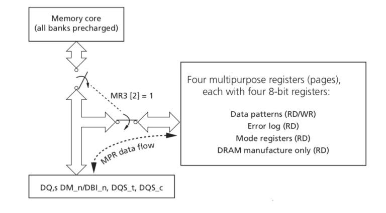
- MR3: Enable MPR (Multi-Purpose Register) mode to prepare for read/write training.
Example: a DDR4-3200 configruation might use CL=16, CWL=14, BL=8, RTT_NOM=240Ω.
Precharge & Refresh:
- Issue PRECHARGE ALL to close active rows in each bank.
- Issue REFRESH to stabilize DRAM cell charge after power-up.
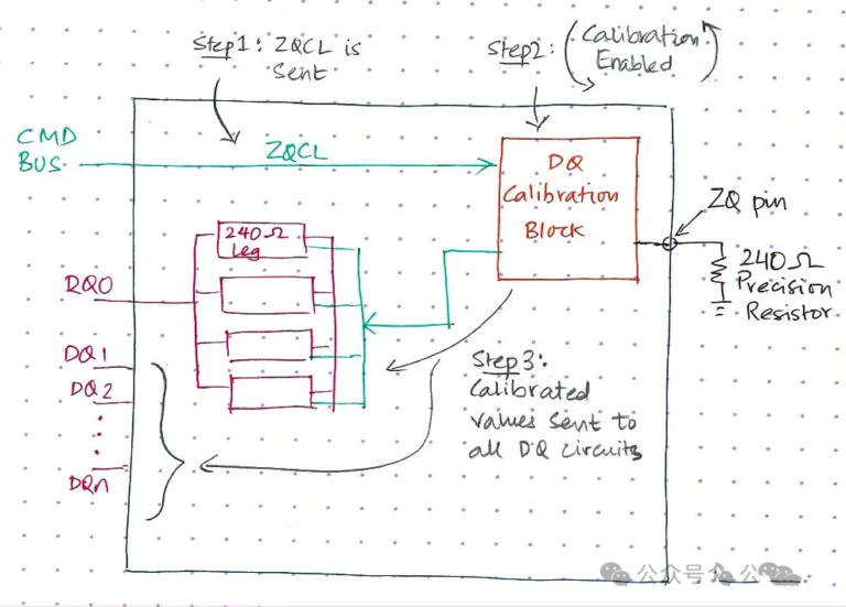
3.2 Phase 2 – ZQ Calibration
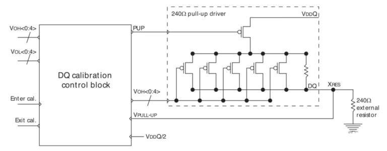
Goal: calibrate DQ drive strength and ODT to match JEDEC target impedance (e.g., 240Ω).
Hardware basis:
- DRAM integrates a ZQ calibration module (comparator and resistor tuning blocks).
- The SSD PCB ties the DRAM ZQ pin to a precision external resistor (e.g., 240Ω ±1%) as a reference.
Calibration flow (ZQCL example):
- Controller issues ZQCL (ZQ Calibration Long) to start full calibration.
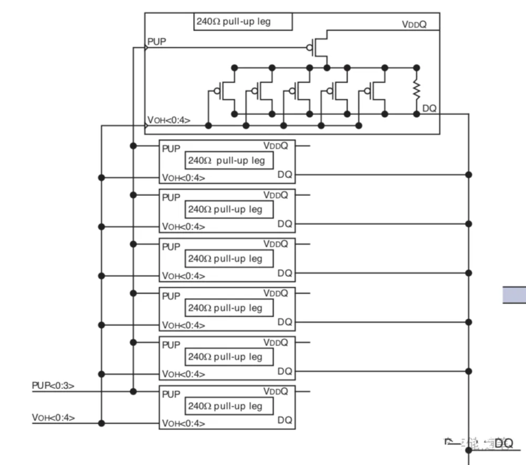
- DRAM’s ZQ module forms a Thevenin divider tith the external ZQ resistor; a comparator adjusts VOH[0:4] (drive strength control bits) until the divider node equals VDDQ/2.
- Calibrated VOH values are applied to the DQ driver circuits.
- Optionally, ZQCS (ZQ Calibration Short) is used for quick runtime recalibration.
Verification:
Post-calibration goals: DQ output impedance error ≤5%; ODT error ≤10%. Engineers typically verify signal reflection coefficients with an oscilloscope (S11) target around |S11| ≤-15dB.
3.3 Phase 3 – VrefDQ Calibration (VrefDQ Training)
Goal: adjust the data sampling reference voltage (VrefDQ) so logic ‘0’ / ‘1’ decisions are robust.
VrefDQ role:
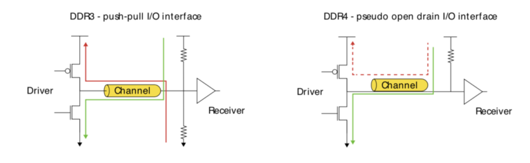
DDR4 uses a pseudo-open-drain interface; receivers lack an internal divider, so VrefDQ defines the decision threshold (commonly between ~0.3VDDQ and 0.6VDDQ). For VDDQ=1.2V, the practical VrefDQ tuning range is roughly 0.36~0.72V.
Calibration flow (2-D sweep method):
- Enter Vref training mode (e.g., via MR6).
- Generate traning patterns (checkerboad 0x55AA/0xAA55 or PRBS).
- Voltage sweep: step VrefDQ in small increments (e.g., 10mV) across the expected range.
- Time/phase sweep: step DQS sampling phase in fine increments (e.g., 1/64 UI) across 0~360°.
- For each (VrefDQ, phase) pair, measure BER and eye area.
- Choose a pair with BER ≤1×10⁻¹² and the largest eye area; store parameters in controller registers.
SSD-specific optimization:
Because NAND activity can couple noise into DDR channels, include simultaneous NAND read/write activity during Vref calibration to ensure the selected VrefDQ remains robust under real workload noise. Reserve ~5~10% margin when choosing operating VrefDQ.
3.4 Phase 4 – Read/Write Training
Goal: align DQS and DQ timing to maximize timing margins for read and write – the most complex stage.
DDR4 provides MPR (Multi-Purose Registers) that are commonly used to store training patterns so that the training process does not occupy NAND cache.
Preparation:
- Enable MPR mode by setting MR3[2]=1.
- Write training patterns into MPR (e.g., MPR0=0xAA, MPR1=0x55, MPR2=0xFF, MPR3=0x00).
- Verify MPR contents via READ back.
Write Training:
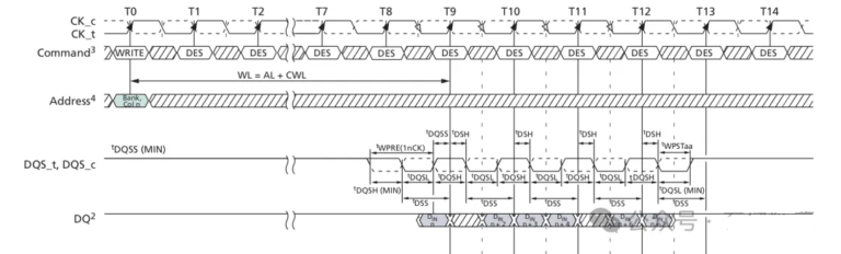
Goal: ensure DQ launched by the controller is sampled correctly by DQS at the DRAM side, satisfying tDQSS (DQS relative to CK) constraints (JEDEC tDQSS ≈0.9~1.1 UI).
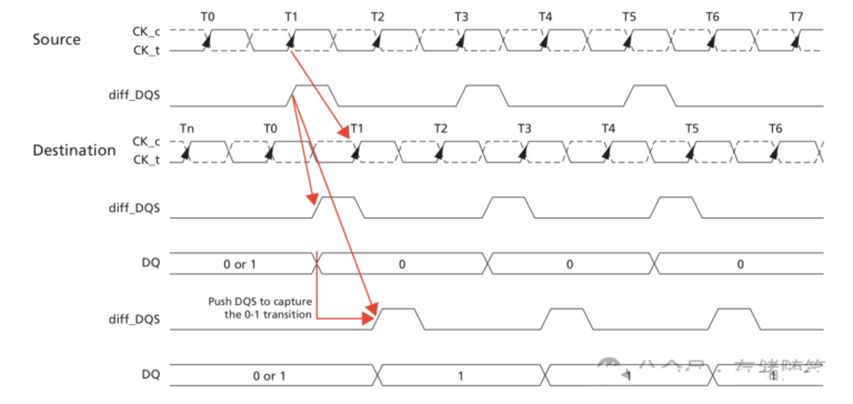
(1) Write Leveling:
- Enable Write Leveling (set MR1[7]=1).
- Controller steps DQS delay (e.g., 1/32 UI steps) while sending SQS pulses.
- DRAM samples CK on DQS rising edges and returns status via DQ.
- Controller locates the critical edge trnsition (feedback from 0->1) to align DQS with CK and locks the DQS delay per DQS group (e.g., for x8 devices DQS0~DQS7).
(2) Write Centering:
- Controller writes alternating patterns (0xAA/0x55) into MPR.
- Sweep DQ-to-DQS delay in fine steps (e.g., 1/64 UI) and read back MPR.
- Record BER at each delay and pick the center of the zero-error window as the optimal write delay so that DQ is centered relative to DQS.
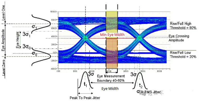
Read Training:
Objective: calibrate the controller/PHY read capture so the sampling point sits at the center of the data eye.
- Enable MPR readback (MR3[2]=1) so DRAM returns MPR patterns during reads.
- Issue continuous reads; DRAM returns stable MPR patterns. Scan internal read delay registers (increment/decrement) to find the left and right eye edges (earliest and latest valid sampling points).
- Center the sampling point between the detected edges and lock the read delay registers.
- Repeat for all DQ bits to complete full-link read centering.
Alternatives / Notese
- Not all implementations use MPR for read centering: older DRAM (e.g., DDR3) lacks MPR and may use direct bank write/read of test patterns. Custom controllers may use proprietary schemes.
- MPR-based centering is a hardware-software cooperative process: firmware initiates/configures training; controller/PHY hardware performs high-speed scanning and edge detection in parallel without software intervening in tight timing loops.
4. Alternatives and Complementary Techniques
- 2-D Vref training: jointly sweep Vref and timing to find the sampling point with the largest eye; commonly used in DDR5/LPDD5 PHYs. It can complement MPR centering (MPR for coarse timing, 2-D Vref for fine tuning).
- Dynamic data-pattern calibration: write PRBS or complex patterns and measure BER during reads to infer optimal timing. This method is slower and consumes memory bandwidth but can be used where MPR is unavailable.
5. Dynamic Considerations and Pos-Training Drift
MPR/static calibration at power-up does not necessarily cover runtime dynamics. Sources of drift include:
- Environmental changes: supply ripple and temperature swings change link delay/impedance.
- Workload variation: heavy DDR activity increases crosstalk and reflections.
- Hardware aging: DRAM driver and PHY delay elements can degrade over time.
Mitigations:
- Periodic re-centering: schedule periodic read-centering (prefer MPR where available) to compensate for environmental drift. Frequency depends on environment (e.g., every 10 minutes in high-temp scenarios; every hour in stable datacenters).
- Adaptive delay compensation: high-end PHYs include VT (voltage-temperature) sensors and dynamically adjust delay registers for milisecond-scale compensation without a full retrain.
- Signal integrity improvements: PCB layout optimization (shorter traces, impedance control), better decoupling, and SerDes-like equalization techniques (Tx FFE / Rx DFE) for high-speed DDR.
- Parameter profiling and dynamic adaptation: sotre calibration profiles for different temperature/load conditions and apply matching parameter sets at runtime to shorten recalibration time.