Address
304 North Cardinal St.
Dorchester Center, MA 02124
Work Hours
Monday to Friday: 7AM - 7PM
Weekend: 10AM - 5PM


Powering the Future of Server Infrastructure
Powering the Future of Server Infrastructure
 Byhyperserver
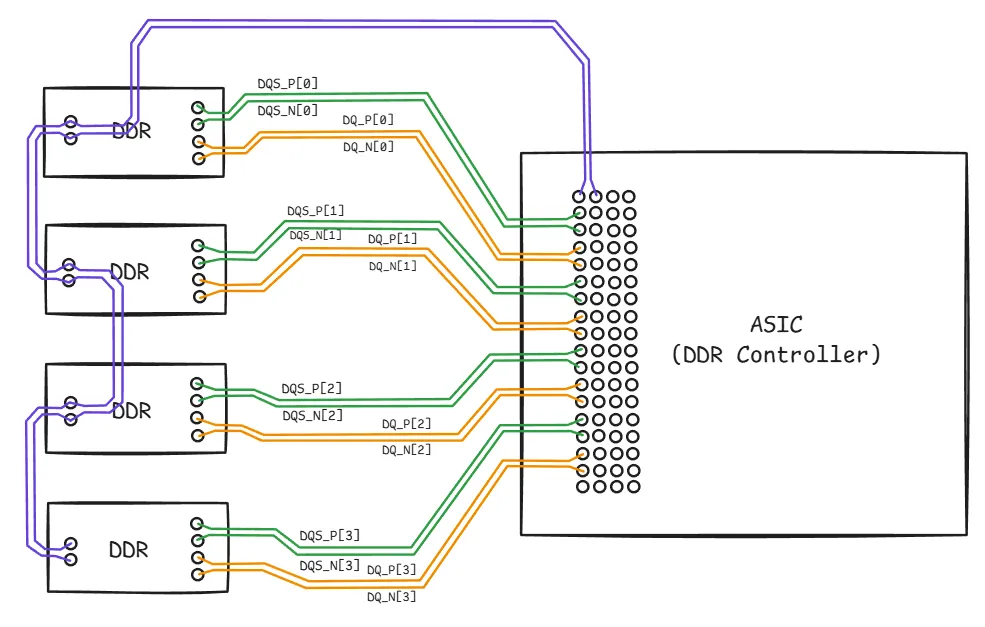
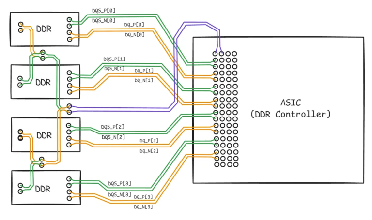
It all starts with PCB routing. Boss Zhao Renfan assigned Xiao Tang a task: to route a DDR3 design. The DQS and DQ signals are relatively easy to route because each DRAM chip has dedicated signals. Soon, Xiao Tang finished routing them (assuming each chip has a 1-bit width):
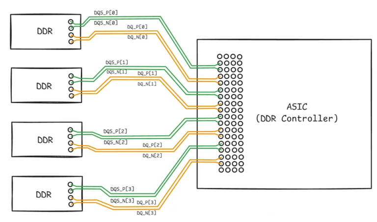
However, the Clock, Address, and Command signals are a bit more troublesome because they are shared by all the chips. So how should they be routed?
The first way is the Double-T topology – one splits into two, and two split into four. The advantage is that the distances from the controller to each DDR chip can be made equal by constraints, so no separate adjustment is needed when operating each chip. However, this topology is not very friendly to signal integrity: the stubs are longer, reflections can be more severe, making it unsuitable for DDR3 or higher-frequency applications.
The second way is Fly-by, i.e., a daisy-chain topology – one chip after another, with termination placed after the last chip.
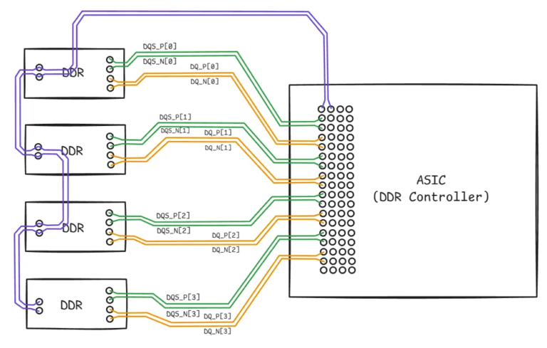
The advantage is improved signal integrity, but the problem is that the distances from the controller to each chip are now different -some are closer, some farther. So how should Clock and Data be sent? If we align to the closest chip, the farther chips will be unhappy (they won’t sample correctly); if we align to the farthest chip, the nearer ones won’t be happy; if we choose a middle point, both sides are dissatisfied.
Just like the common issues faced by any large organization, group, or society, not every policy or decision can satisfy everyone. However, unlike those organizations, which can sacrifice the interests of a minority to please the majority, the DDR controller cannot do that – it must satisfy all chips, otherwise the entire systme will not work properly.
What to do then?
This is where Write Leveling comes in.
The purpose of Write Leveling is to ensure that when the DQS signal reaches each DRAM chip, its rising edge is aligned with the rising edge of the clock (CK).
How is it done?
A simple animated illustration is provided below for referance.
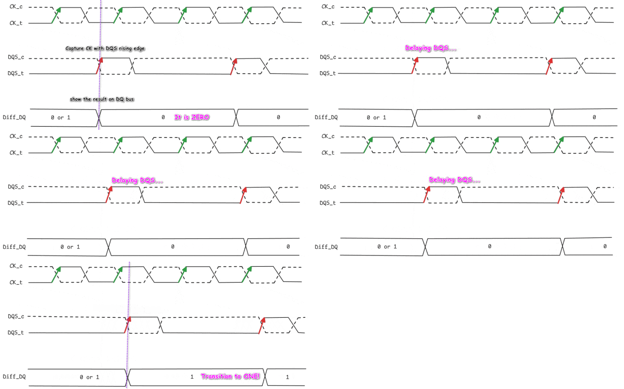
DDR data (DQ) is sampled using the DQS signal, not CK. So why does DQS still need to be aligned with CK? As long as DQS and DQ are aligned, shouldn’t the sampled data be correct?
The main reason is that the operation requires cross-clock domain handling. The data on DQ is not merely sampled and done – it must be stored into the memory cell, and that internal logic circuitry is driven by CK, not by DQS. Therefore, if DQS and CK are not aligned, the internal logic cells may capture incorrect data.
You, being clever, have surely already thought of this: Write Leveling only gurantees that the rising edges of DQS and CK are aligned, but it does not determine which rising edge of CK is aligned with DQS.
For example:
Suppose that when sent from the controller, DQS and CK are aligned as follows:

After arriving at the DDR chip, because the DQS trace is usually shorter than the CK trace, DQS often reaches the chip earlier than CK. Their relationship may look like this:

After Write Leveling, DQS is delayed and will align with the T-1 cycle of CK, as shown below:

In this case, although DQS and CK are rising – edge aligned, they are already ooset by one cycle, which will also cause data errors.
What to do then?
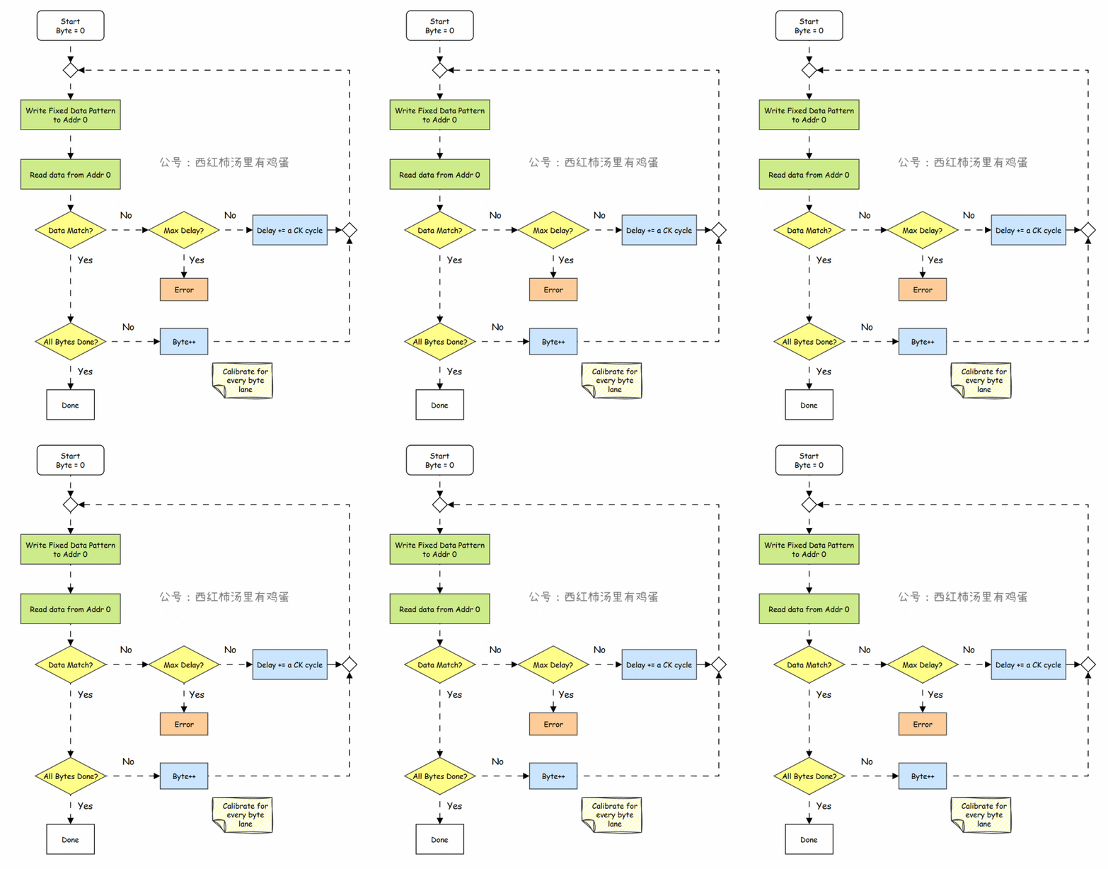
This can be resolved throught Write Latency Calibration. The core approach is : the DDR controller writes a fixed pattern of data into the DDR chip, reads it back and checks. If the result is not as expected, it delays DQS one cycle and repeats until the data is correct. The flowchart is as follows: