Address
304 North Cardinal St.
Dorchester Center, MA 02124
Work Hours
Monday to Friday: 7AM - 7PM
Weekend: 10AM - 5PM

Powering the Future of Server Infrastructure
Powering the Future of Server Infrastructure


NVIDIA HGX B300 8-GPU System Block Diagram
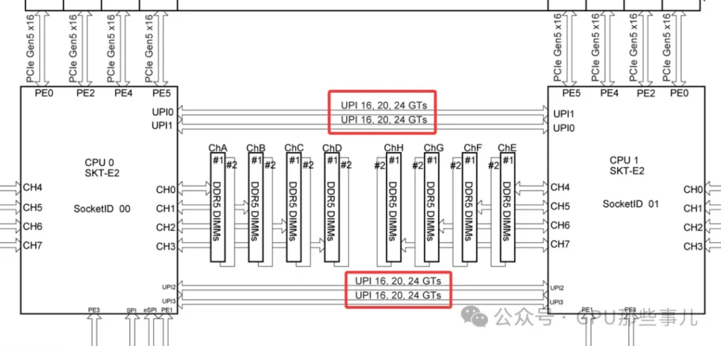
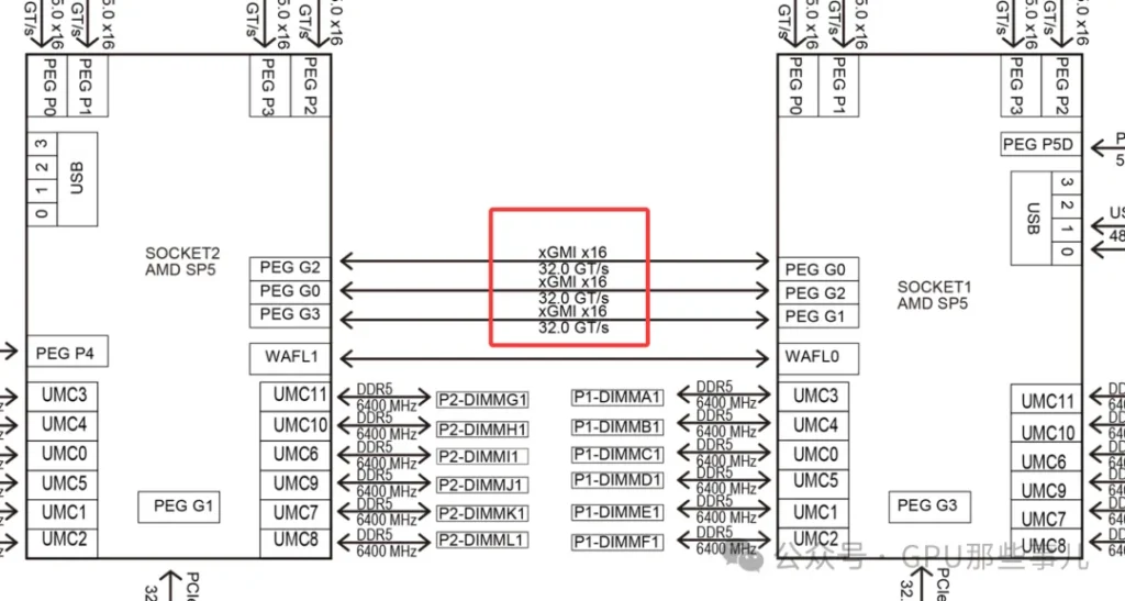
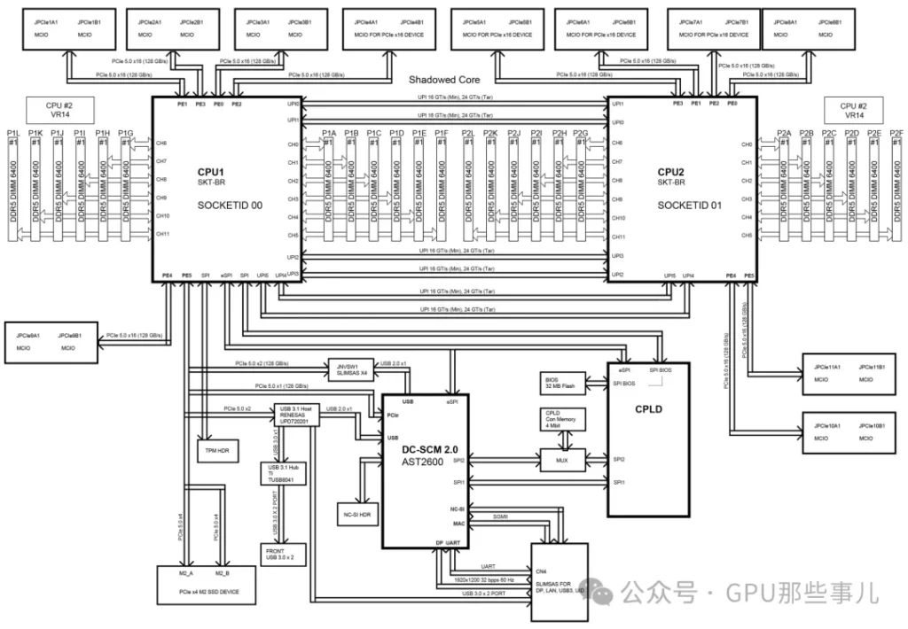
CPUs are connected by a dedicated high-speed interconnect bus. This interconnect typically does not consume the PCIe lanes available for external devices, but it does use up internal bus resources on the CPU.
The interconnect technology depends on the CPU vendor and platform. Modern mainstream server interconnect technlogies include Intel’s Ultra Path Interconnect (UPI), and AMD’s Infinity Fabric.
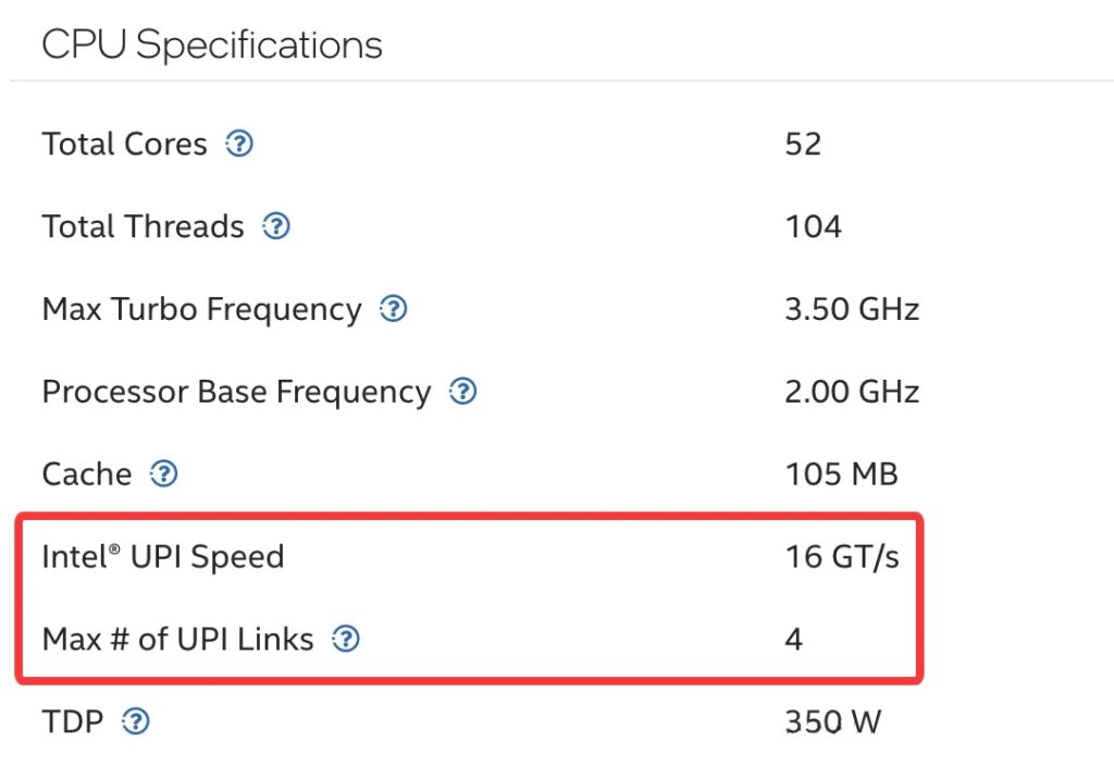
Intel® Xeon® CPU Max 9470 Processor specifications
Partial motherboard view of an NVIDIA HGX B300 8-GPU system (Intel platform)
某厂Partial motherboard view of an NVIDIA HGX B300 8-GPU AMD system (AMD platform)
Common characteristics: These technologies are ultra-high-speed, low-latency buses specifically designed for CPU-to-CPU communication. They far exceed the PCIe standard of their era in performance and are used to transimit critical data such as cache coherence traffic and memory accesses.
1)No consumption of “user-avaiable” PCIe lanes:
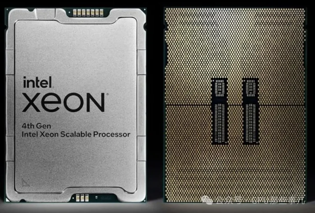
Intel Xeon CPU Max 9480
2)Consumes CPU internal resources and physical pins:
The key challenge in GPU server PCIe lane allocation is ensuring GPUs are “plugged into the right slots” and that software “runs on the right CPU”, to avoid data traveling long distances over the CPU interconnect bus. This is critical for extracting the maximum performance from the system.
1)Dual-CPU NUMA architecture: After connecting two CPUs, the system forms a NUMA (Non-Uniform Memory Access) architecture. PCIe lane allocation across the system is strictly constrained by this NUMA setup. Key points include:
2)When configuring a dual-socket server, it is crucial for optimal performance to place device (GPUs, high-speed NICs, etc.) in appropriate slots and bind processes to the correct CPU. This ensures that most memory and I/O traffic stays local to each CPU.
1)In a dual-CPU system, each CPU’s PCIe lanes are independent and only available locally. This is a key consideration.
2)Resource distribution (for example, suppose each CPU provide 48 PCIe 5.0 lanes):
3)GPU Inserts performance differences:
Block Diagram of an HGX H200 NVL server motherboard
1)Check the motherboard manual: Before assembling or deploying a GPU server, consult the motherboard manual’s Motherboard Block Diagram and Motherboard Layout. These diagrams clearly indicate which CPU each physical slot is connected to.
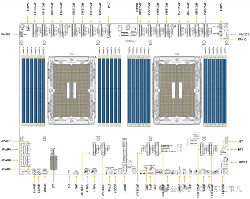
HGX H200 NVL server Motherboard Layout
2)Balance load and optimize paths:
3)Use NUMA-aware tools: On Linux systems, use tools such as numactl, lstopo, etc., to view the NUMA topology. When launching tasks, bind the CPU and memory nodes appropriately to keep workloads and data local.
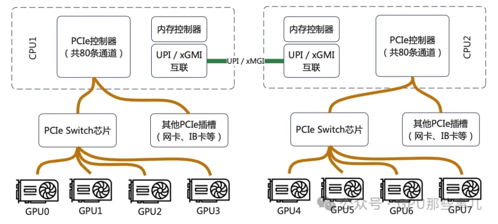
PCIe Switch cannot increase the total number of physical lanes provided by the CPUs. Their core function is to “redistribute and aggregate” these lanes to address key issues in GPU deployments, such as topology flexibility and maintainability.
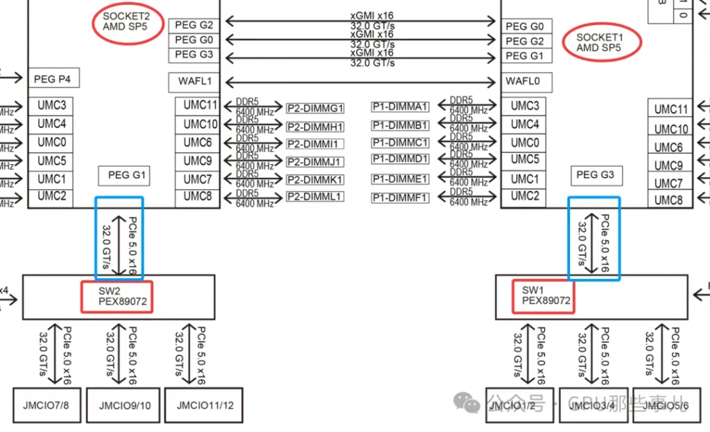
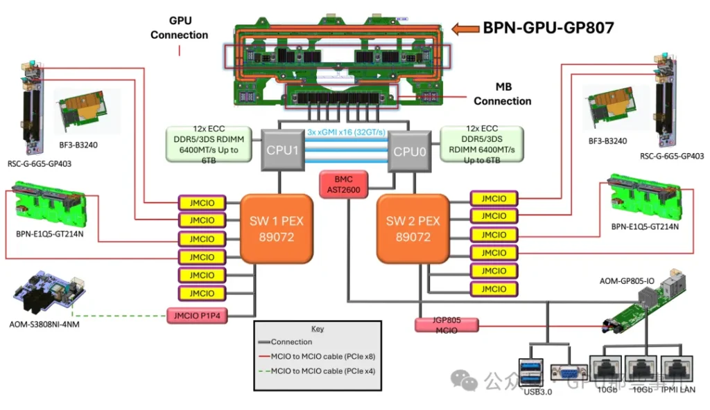
某厂Partial motherboard view of an NVIDIA HGX B300 8-GPU system (AMD platform) with dual PCIe Switch (PEX89072)
1)Each CPU’s PCIe lanes come out though a limited number of physical interfaces (e.g., a few x16 slots). Without a switch:
2)Role of PCIe Switch: The sitch allows a set of CPU lanes (for example, 16 PCIe lanes) to be “expanded” by the switch chip ointo multiple x16 downstream interfaces (e.g., 8×16 ports), although those eight ports share the bandwidth of the original 16 upstream lanes. More importantly, the switch can intelligently configure connectivity among its downstream ports. This provides an ideal, structured physical wiring foundation for NVLink interconnects between GPUs. In HGX motherboards, this complex combination of PCB routing and switch logic implements full of partial NVLink topologies among the GPUs.
1)CPU lane shortage: In an 8-GPU server configuration, a fundamental problem is that no singel CPU can supply enough PCIe lanes to coneect all 8 GPUs (each GPU typically needs x16 lanes).
2)Switch solution (example of a typical 8-GPU HGX):
1)Hot-plug support: PCIe Switch typically provide better hot-plug (hot-swap) support, which is essential in high-availability data centers.
2)Bandwidth management and Qos: A switch can manage downstream GPU PCIe traffic with priority controls (like a network switch), preventing one GPU’s burst traffic from blocking the communication of others.
3)Fault isolation: If a downstream link or GPU fails, the switch can iolate the fault to some extent, preventing it from affecting the entire PCIe hierarchy.
In integrated AI servers like NVDIA HGX, the PCIe switch is a critical “enabling” component. It cannot magically create more PCIe lanes, but it redistributes and challenges of topology, flexibility, scalability, and manageability in large-scale, can operate at optimal performance. The introducation of the PCIe switch is a key step in evolving servers from “multiple independent GPUs” to an “integrated AI compute unit”。
In high-end GPU servers (such as NVIDIA HGX, DGX, and various OEM 8-GPU system), the allocation of PCIe lanes from CPUs to the PCIe Switch is a carefully balanced design choice that directly affects system performance and cost.
1)A typical dual-socket high-end GPU server is usually based on:
2)Common allocation patter: Each CPU allocates 32 or 48 PCIe lanes to the PCIe switch that connect to the GPUs.
Let’s check a specific and typical diagram of PCIe lanes allocations based on Intel platform (dual 4th/5th Xeon) 8-GPU server :
其The core design principle is not to maximize the bandwidth of any single GPU, but to ensure that all GPUs can simultaneously and evenly access noth CPUs and the entire system memory, thus maximizing aggregate bandwidth.
1)Balance principle (core): Ensure each GPU can efficiently access either CPU and its local memory in a peer-to-peer manner. 这This optimizes NUMA performance. If all lanes originate from one CPU, GPUs under the other CPU would have only “remote” memory access with much higher latency. Therefore, typically both CPUs contribute equal numbers of lanes to the switch (for example, 32 lanes each for 48 lanes each).
2)Separation of direct and switched paths:
3)Aggregate bandwidth matching principle: The total uplink bandwidth allocated to the switch (for example, dual sockets each providing 48 lanes of PCI 4.0=2x48x2GB/s ≈ 192 GB/s) should match the GPUs’ aggregate demand on system memory and network bandwidth. In design, ensure that the network is not the bottleneck. For instance, when 8 H100 GPUs synchronize via NVLink, the place tremendous load on CPU menory accesses; sufficient uplink PCIe bandwidth is required to “feed” them.
4)Topology optimization principle: The allocation scheme should be co-designed with the GPU interconnect topology (NVLink). In HGX designs, the placement of PCIe switches and the uplink bandwidth allocation are agrranged to complement NVLink switches, allowing GPUs to inter-communicate at high speed via NVLink while also communicating efficiently with CPUs, memory, and network though balanced PCIe uplinks.
NVIDIA HGX B300 8-GPU System Block Diagram
1)This is the most important trade-off:
2)Example solutions:
In professional GPU servers, the number of lanes a CPU assigns to the PCIe switch is not a fixed value, but the result of a system-level design. The goal is to achieve the best bandwidth balance among GPUs, CPU memory, high-speed network, and storage, while also meeting the GPU’s need for peer access and low-latency communication. In typical dual-socket 8-GPU systems, allocating 32 or 48 lanes per CPU to the GPU switch has been validated as the “sweet spot” solution for optimizing overall performance.