Address
304 North Cardinal St.
Dorchester Center, MA 02124
Work Hours
Monday to Friday: 7AM - 7PM
Weekend: 10AM - 5PM


Powering the Future of Server Infrastructure
Powering the Future of Server Infrastructure
 Byhyperserver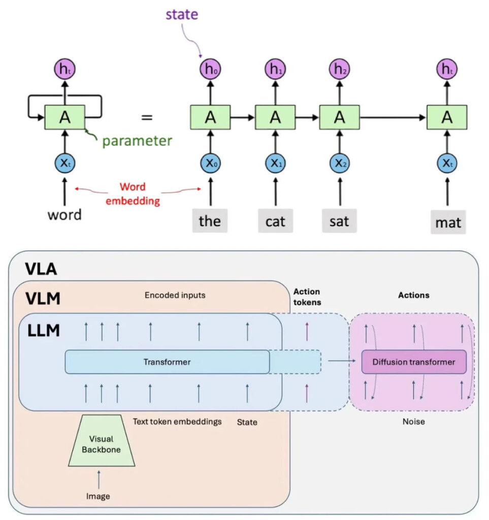
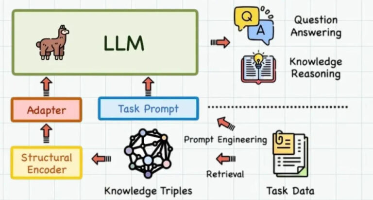
Representatives: GPT series, Claude, LLaMA, DeepSeek-V3, Kimi K2, GLM-5.
The undisputed core model type, based on the Transformer architecture and trained on massive text corpora, its core task is to predict the next token. ChatGPT, Claude, Gemini, Kimi, and DeepSeek are all built on top of it. Nearly all AI products rely on an LLM as their foundation.
Capabilities are improved by increasing parameter scale, including layers, attention heads, and MLP dimensions. GPT(Generative Pre-trained Transformer) is a classic subclass of LLM rather than a synonym.
LLM is the general term for large language models, while GPT specifically refers to the autoregressive + pretraining + Transformer paradigm.
Most modern LLMs are built on a Decoder-Only architecture. By using a Causal Attention Mask, they generate tokens autoregressively from left to right, which is the foundation of their powerful generation capabilities.
Representatives: Mixtral, DeepSeek-V3, Kimi K2/K2.5, GLM-5, LLaMA 4.
Strictly speaking, MoE is not an independent model category but an architectural strategy.
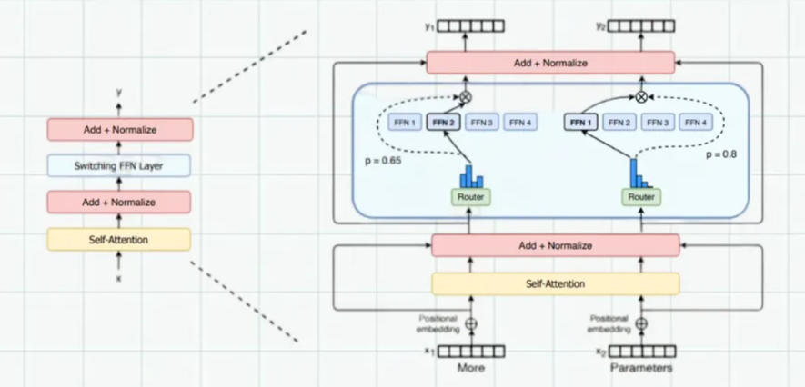
The core idea is to split the FFN (feed-forward network) inside a Transformer block into dozens or even hundreds of expert subnetworks. During each inference step, only a small number of experts are activated through a router.
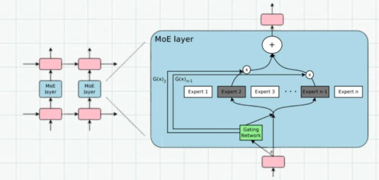
The advantage is that the total parameter count can become extremely large while the computation required for a single inference remains comparable to a small model.
For example, DeepSeek-V3 has 685B total parameters but activates only 37B during inference.For instance, Kimi K2.5 contains 1T parameters in total, while only 32B parameters are activated during inference (8 experts selected from a pool of 384). Likewise, GLM-5 has 744B parameters, with only 44B activated per inference request.
MoE is widely regarded as one of the most practical architectural solutions for achieving an optimal balance between model capability and inference efficiency. In this area, Chinese foundation models have demonstrated leading engineering expertise and innovation.
Representatives: CLIP, SigLIP, Flamingo, InternVL.
VLM is the first step for LLMs toward multimodality: enabling models to understand both images and text. The core idea is to use contrastive learning (such as CLIP) or cross-attention mechanisms to map images and text into the same embedding space, enabling the model to understand the semantic meaning of images.
VLMs themselves typically do not focus on text generation. Instead, they are mainly used for alignment tasks such as image-text matching, zero-shot classification, and image retrieval. Their true value lies in providing key components for subsequent MLLMs. Nearly all Vision Encoders used in modern MLLMs (such as ViT and SigLIP) originated from VLM research field.
VLM can be regarded as the ‘eyes’ of an MLLM. Although many of its capabilities have been absorbed into MLLMs, visual-language alignment remains a highly active research field.
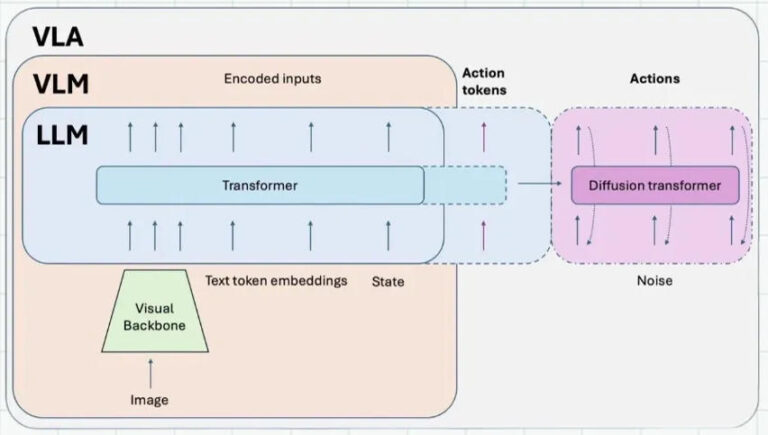
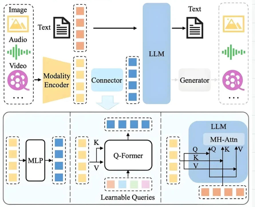
Representatives: Gemini, GPT, Claude, Kimi K2.5, and GLM. A major focus of AI development in 2025. Built upon LLMs, MLLMs can simultaneously understand multiple modalities including text, images, video, audio, and structured data.
There are two primary implementation approaches. The first is attached modality adapters (Vision Encoder + Projection Layer) to an existing LLM, mapping non-text inputs into the LLM’s embedding space.
The second is multimodal joint pretraining from scratch, enabling the model to natively understand cross-modal relationships. Kimi K2.5 follows this approach by jointly training on mixed visual and text tokens.
Modern MLLMs can not only understand images and videos but also generate images (such as the built-in image generation capabilities of ChatGPT and Gemini) and videos (such as Sora).
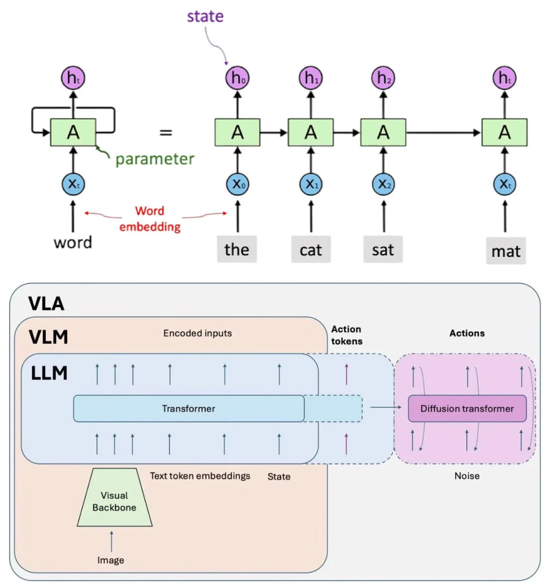
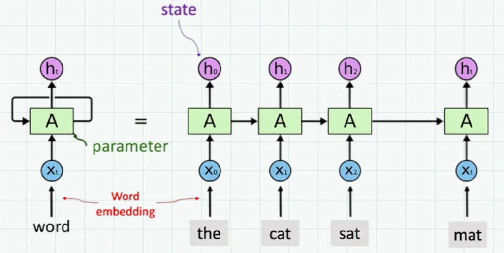
Before Transformers, RNNs dominated sequence modeling. Their core principle is to process sequence data step by step, feeding both the current input and the previous hidden state into the network. This hidden state serves as the model’s memory.
LSTM and GRU mitigated the vanishing-gradient problem of traditional RNNs through gating mechanisms (forget gates, input gates, etc.), and once dominated machine translation, speech recognition, text generation, and nearly all NLP tasks.
However, RNNs have two major limitations: first, their sequential computation cannot be easily paralleized, resulting in low training efficiency; second, the hidden state is a fixed-dimensional vector, causing information to be compressed and overwritten in long sequences, which weakens long-range dependency modeling.
These two bottlenecks directly led to the emergence of the Transformer architecture in 2017. By leveraging self-attention, Transformer largely replaced RNNs. Today, RNNs are no longer used in mainstream LLMs, but they still have a role in resource-constrained sequential tasks such as sensor data processing and embedded systems.
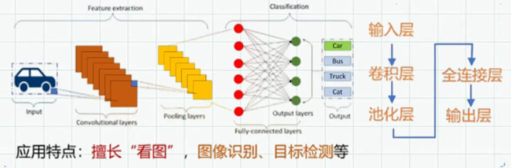
Before Transformers, CNNs dominated computer vision. Their core idea is to use convolution kernels to scan images and automatically learn hierarchical visual features ranging from low-level patterns (edges and textures) to high-level concepts (objects and scenes), without requiring manually designed feature extractors.
In 2012, AlexNet dramatically outperformed traditional methods on ImageNet, ushering in a golden decade for deep learning. Later, ResNet used residual connections to scale networks to 152 layers, conclusively demonstrating that deeper that deeper networks could achieve stronger performance.
CNNs faced challenges similar to RNNs: their local receptive fields limited the capture of global information, wheras Transformer’s self-attention naturally models relationships between any positions. The emergence of Vision Transformer (ViT) gradually displaced CNNs in high-accuracy vision tasks.
Howerver, CNNs still possess an advantage that Transformer have not fully replaced: low computational cost and fast inference. Architectures such as MobileNet and EfficientNet are highly optimized for mobile phones and edge devices, and remain dominant in latency-sensitive applications such as real-time detection and mobile deloyment.